
When you hold a smartphone or a computer chip, you might not think about where it came from. Each chip originates from a 300 mm (12-inch) round silicon wafer. But how many chips can a single wafer produce? The answer is simple in theory, yet full of fascinating geometry, physics, and engineering details.
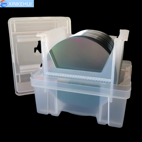
From Circle to Square: A Mathematical Puzzle
A 300 mm wafer has a radius of 150 mm, giving it an area of roughly 70,685 mm². If each chip is 10 mm × 10 mm, the wafer could theoretically contain about 706 chips.
However, wafers are circular while chips are square. This mismatch creates edge losses, meaning not all of the wafer area can be used. After accounting for these losses, only about 85–90% of the theoretical maximum is typically usable. In practice, a 300 mm wafer produces roughly 600 usable chips of that size.
If the chip is smaller, say 5 mm × 5 mm, the wafer can hold approximately 2,400 chips. Smaller chips increase output, but also raise challenges in cutting precision and defect management.
Yield Matters: Not Every Chip Makes It
Even after cutting, each chip undergoes testing and quality control. Edge chips or those with micro-defects may be discarded. Typical yield rates range from 80–95%, which further reduces the number of chips that reach the market.
Thus, the final chip count from a 300 mm wafer depends on chip size, cutting precision, manufacturing process, and yield. A single wafer can produce anywhere from several hundred to several thousand chips, depending on these factors.
Industrial Wonder: Small Wafer, Huge Impact
It’s remarkable that a wafer just 12 inches in diameter can produce thousands of chips, which form the backbone of modern electronics—smartphones, computers, servers, electric vehicles, and even spacecraft.
Inside a semiconductor fab, wafers undergo photolithography, etching, doping, and metallization before becoming individual chips. Every step pushes the limits of geometry and materials science to maximize output, ensure performance, and minimize defects.
Conclusion
A 300 mm / 12-inch silicon wafer is more than a piece of material—it is a showcase of engineering and mathematics. From circular wafer to square chips, every step demonstrates precision, optimization, and innovation. Next time you hold a device, remember: its brain may come from a wafer barely one foot across, yet capable of producing hundreds or thousands of intelligent chips.