
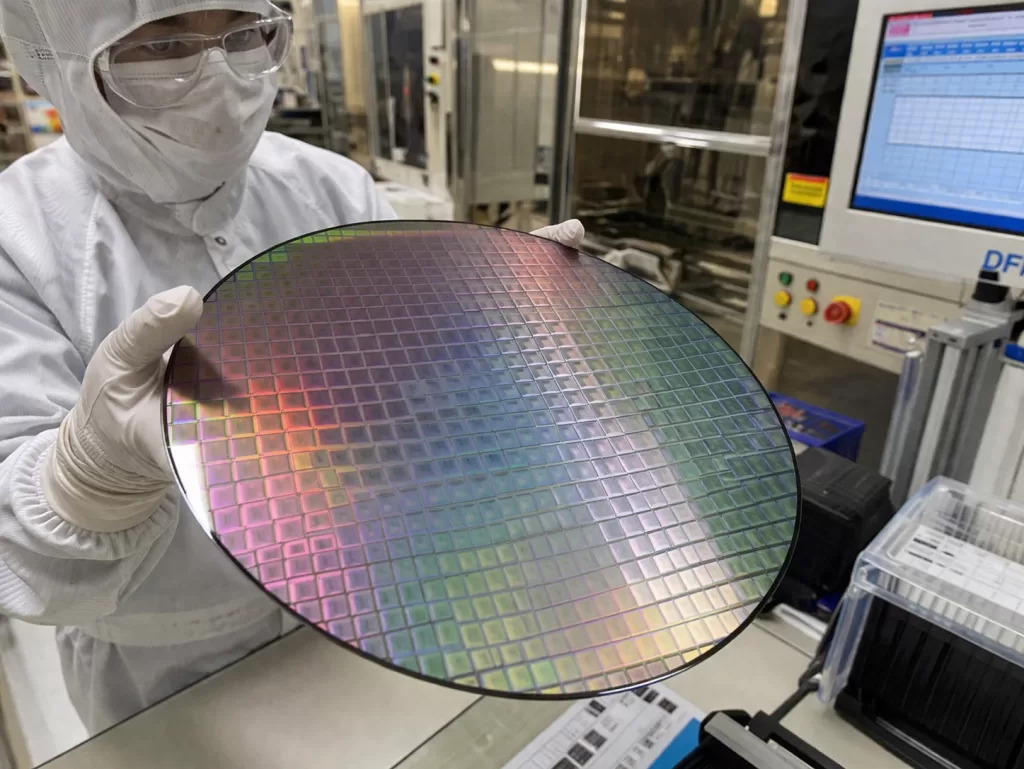
The production of modern microprocessors, such as Intel’s Skylake series, starts with large silicon wafers. Understanding how many chips a single wafer can yield is crucial for semiconductor manufacturers, hardware designers, and industry analysts. In this article, we will examine the factors that determine the number of Skylake chips produced from a standard 300mm (12-inch) silicon wafer, using industry best practices.
1. Introduction to Skylake Architecture
Skylake is Intel’s 6th-generation Core microarchitecture, introduced in 2015. It is manufactured using 14nm FinFET technology, supporting multiple cores, Hyper-Threading, and integrated graphics. Depending on the model, a Skylake processor can range from a dual-core mobile chip to a quad-core or hex-core desktop CPU, with die sizes typically between 122 mm² and 151 mm².
The die size of a chip is critical because it directly affects the number of chips that can be produced from a single wafer.
2. Understanding Wafer Yield
A 300mm silicon wafer is standard in modern semiconductor fabrication, offering high throughput and lower cost per chip. However, the total number of chips per wafer depends on several factors:
- Die Size – Larger dies occupy more wafer area, reducing the total number of chips.
- Wafer Edge Losses – Dies near the circular edge of the wafer are often unusable.
- Defect Density – Not all dies are functional due to fabrication defects.
- Process Complexity – More complex designs may lower yield slightly.
3. Estimating the Number of Chips per Wafer
To estimate the number of chips per wafer, follow these steps:
- Calculate the wafer area: The area of a 300mm wafer is approximately 70,685 mm² (using the formula for the area of a circle: π × radius², where the radius is 150mm).
- Account for edge losses: About 10% of the wafer area is typically unusable near the edges. The usable area is then approximately 63,617 mm².
- Divide by die size: For a standard Skylake desktop CPU with a die size of 145 mm², divide the usable wafer area by the die size: 63,617 ÷ 145 ≈ 438 chips.
- Factor in manufacturing yield: With typical yields of 85–90%, the number of functional chips per wafer is approximately 372–394.
Note: Smaller Skylake mobile dies may produce over 500 chips per wafer, while larger high-end desktop or server dies may produce fewer than 350 functional chips.
4. Why This Calculation Matters
- Cost Analysis: Wafer yield directly impacts the manufacturing cost per chip. Higher yields reduce cost and increase profitability.
- Supply Chain Planning: Knowing potential output helps manufacturers plan production volumes and inventory.
- Technology Scaling: As semiconductor nodes shrink (for example, 10nm and 7nm), die sizes decrease, allowing more chips per wafer, but process complexity may affect yields.
5. Real-World Considerations
- Variation Across Models: Mobile Skylake chips are smaller, producing more dies per wafer than desktop or server variants.
- Defective Dies: Some dies fail quality checks and are unusable or sold as lower-tier products.
- Future Trends: The industry is moving toward larger wafers (450mm) and advanced packaging, which could increase output per wafer significantly.
6. Conclusion
Estimating the number of Skylake chips on a 300mm wafer involves geometry, yield statistics, and real-world defect analysis. For standard desktop Skylake dies (~145 mm²), a single 300mm wafer can produce approximately 372–394 functional chips. Understanding this metric is crucial for cost modeling, production planning, and forecasting in the semiconductor industry.
With advancements in wafer technology and lithography, future generations of CPUs will see higher yields and more efficient manufacturing, continuing the rapid pace of computing innovation.