
Semiconductor wafers become increasingly fragile as they are thinned for power devices, RF components, MEMS, advanced packaging and compound-semiconductor applications.
A thin wafer may crack, warp or become impossible to handle without temporary mechanical support. The device wafer is therefore bonded to a rigid carrier before backgrinding, polishing, etching, metallization or dicing.
Sapphire carrier wafers are considered for these applications because they provide:
- High mechanical stiffness
- Good dimensional stability
- High hardness
- Optical transparency
- Chemical resistance
- High-temperature capability
- Cleanroom-compatible polished surfaces
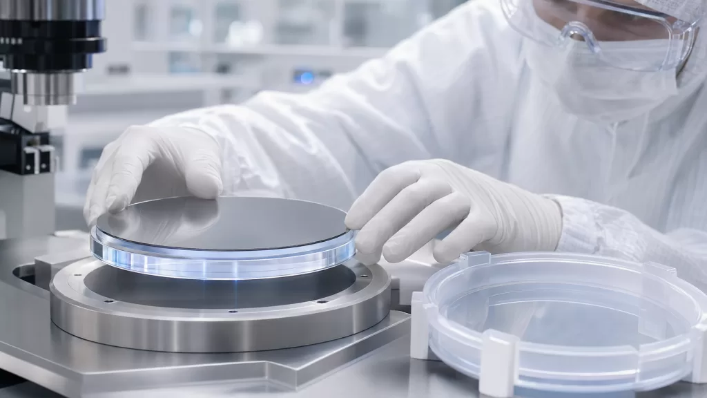
However, choosing sapphire only by diameter and thickness is not sufficient. Carrier flatness, coefficient of thermal expansion, adhesive compatibility, surface condition and debonding method can all affect the bonded stack.
Buyers must also define when a used carrier can safely return to production. There is no universal statement such as “a sapphire carrier can be reused ten times.” Reuse should be determined through inspection and requalification.
Why Thin Wafers Need a Carrier
Wafer thinning may reduce electrical or thermal resistance, enable smaller packages, improve heat dissipation or expose through-wafer structures.
The process may include:
- Backgrinding
- Lapping
- CMP polishing
- Wet etching
- Dry etching
- CVD or PVD deposition
- Electroplating
- Backside metallization
- Lithography
- Laser processing
- Dicing
As thickness decreases, the wafer loses bending stiffness and becomes more sensitive to handling stress.
Temporary bonding attaches the device wafer to a rigid carrier with a removable adhesive system. The carrier supports the wafer from thinning through downstream processing and is removed after the backside work is complete.
This support process is widely used for fragile compound-semiconductor and advanced-packaging wafers.
What Is a Sapphire Carrier Wafer?
A sapphire carrier wafer is a polished single-crystal Al₂O₃ wafer used as a temporary or, in selected applications, permanent mechanical support.
The bonded stack normally contains:
- Device wafer
- Temporary bonding adhesive or release layer
- Sapphire carrier wafer
The carrier may have the same nominal diameter as the device wafer or be slightly oversized to simplify edge support and handling.
Commercial sapphire carrier products may be supplied in customized diameters such as 104 mm for selected 4-inch processes or 156–159 mm for 6-inch processing. Thickness and SSP/DSP surface conditions can also be customized.
Applications of Sapphire Carrier Wafers
Sapphire carriers may support:
- Silicon wafers
- GaAs wafers
- GaN wafers
- SiC wafers
- InP wafers
- MEMS substrates
- Optical wafers
- Sensor wafers
- Thin-film devices
- Fragile ceramic substrates
Typical applications include:
- GaAs wafer thinning and polishing
- Power-device backside processing
- RF-device substrate thinning
- Laser lift-off
- Thin-wafer transfer
- Temporary bonding and debonding
- Backside metallization
- Dicing support
- Research sample preparation
Why Flatness Is Critical
The carrier provides the geometric reference for the complete bonded stack.
If the carrier has excessive bow, warp or thickness variation, the bonded device wafer may not remain uniformly supported.
Possible consequences include:
- Non-uniform grinding thickness
- Local over-grinding
- Bond-line thickness variation
- Trapped voids
- Lithography focus errors
- Chucking problems
- Wafer-handling alarms
- Edge lifting
- Delamination
- Cracking during debonding
Flatness should therefore be evaluated through several separate parameters.
TTV, Bow and Warp Explained
Total Thickness Variation
TTV is the difference between the maximum and minimum measured thickness across the wafer.
A low carrier-wafer TTV helps maintain a uniform bonded-stack thickness during grinding and polishing.
However, final stack TTV also depends on:
- Device-wafer geometry
- Adhesive thickness
- Adhesive flow
- Bonding pressure
- Bonding temperature
- Surface topography
- Trapped particles
A low-TTV carrier cannot compensate for a non-uniform adhesive layer.
Bow
Bow describes the displacement of the wafer’s center relative to a reference plane in an unclamped condition.
Excessive carrier bow can make vacuum chucking, alignment and bonding difficult.
Warp
Warp describes the overall peak-to-valley deviation of the wafer surface from a reference plane.
A carrier may have acceptable TTV but excessive warp. Both parameters should therefore appear in the RFQ.
Local Flatness and Edge Roll-Off
Global measurements do not always identify local high or low regions.
Processes involving direct bonding, lithography or very thin final wafers may also require:
- Local thickness variation
- Site flatness
- Edge roll-off
- Surface waviness
- Full-wafer geometry mapping
Typical Sapphire Carrier Flatness Specification
The required limits depend on carrier diameter, thickness, bonding method and final device-wafer thickness.
An example RFQ may include:
- Carrier diameter: 156 or 159 mm
- Thickness: 0.5–1.0 mm
- TTV: less than 5 µm
- Bow and warp: buyer-defined maximum
- Surface roughness: Ra below 0.5 nm on the bonding side
- Parallelism: buyer-defined
- Edge profile: smooth rounded or beveled edge
- Edge chips and cracks: none within agreed limits
These values are an example rather than a universal industry standard.
The carrier should be specified according to the bonded-stack and equipment requirements, not only the carrier’s standalone datasheet.
SSP or DSP Sapphire Carrier?
Single-Side Polished Carrier
An SSP carrier has one polished surface and one ground, lapped or less-finely finished surface.
SSP may be suitable when:
- Only one bonding surface is required
- Backside optical transmission is not critical
- The equipment can handle the backside finish
- Cost reduction is important
Double-Side Polished Carrier
A DSP carrier has polished front and back surfaces.
DSP may be preferable for:
- Through-carrier optical inspection
- Laser debonding
- Double-side alignment
- Interferometric flatness measurement
- Low-particle handling
- Processes requiring controlled backside contact
- Carrier reuse
The backside finish must also be compatible with vacuum chucks and robotic handling. An excessively rough backside may generate particles, while an extremely smooth backside may affect chucking or sticking in some processes.
Bonding Compatibility Is a Complete System Property
A sapphire carrier should not be evaluated separately from the adhesive and debonding technology.
The complete system includes:
- Device-wafer material
- Sapphire carrier
- Adhesive
- Release layer
- Surface treatment
- Bonding tool
- Thermal process
- Chemical exposure
- Debonding equipment
- Cleaning process
Temporary bonding materials must withstand grinding, thermal cycling, wet processing and deposition without excessive flow, voiding or delamination. They must still allow the carrier to be removed without damaging the thin device wafer.
Common Temporary Bonding Methods
Thermoplastic Adhesive Bonding
A thermoplastic material is applied to the device wafer or carrier and softened during bonding.
Advantages include:
- Good feature-filling capability
- Compatibility with thermo-compression bonding
- Possibility of thermal slide debonding
- Solvent cleaning after separation
The adhesive must retain sufficient mechanical strength at the maximum downstream temperature.
Thermoset or Curable Adhesive
The adhesive is cured after the wafers are brought into contact.
Advantages may include:
- Strong bond stability
- Resistance to high process temperatures
- Good support for high-topography surfaces
The debond and residue-removal processes must be validated carefully.
Wax Bonding
Wax systems are used in selected grinding, polishing and optical-processing applications.
They can be economical but may have more limited thermal stability or contamination control than advanced semiconductor temporary-bonding materials.
Laser Debonding
A laser-sensitive layer or adhesive is irradiated through a transparent carrier.
Sapphire transparency can support this approach, but transparency alone does not guarantee compatibility.
Buyers must confirm:
- Laser wavelength
- Sapphire transmission at that wavelength
- Carrier thickness
- Surface coatings
- Adhesive absorption
- Release-layer design
- Laser focus
- Residue after debonding
Temporary debonding systems may use near-infrared, visible or ultraviolet wavelengths depending on the material platform.
Mechanical Debonding
The carrier is separated at a controlled release interface using low mechanical force.
This method requires:
- Predictable interfacial adhesion
- Good carrier-edge quality
- Low-force crack initiation
- Support for the thin device wafer
- Controlled peel or separation geometry
Thermal Slide Debonding
The adhesive is heated above its softening temperature, and the device wafer and carrier are separated through a controlled lateral movement.
Carrier thickness and stiffness must be sufficient to resist bending during the slide process.
Coefficient of Thermal Expansion Compatibility
Sapphire offers high-temperature stability, but its CTE may not match every device-wafer material.
During heating and cooling, a CTE mismatch can create:
- Bonded-stack bow
- Interfacial shear stress
- Edge lifting
- Adhesive deformation
- Wafer cracking
- Delamination
The adhesive can absorb some stress, but it cannot eliminate a large mismatch under every process condition.
Research comparing sapphire carriers with CTE-matched glass carriers for SiC backside processing found that matched glass could produce lower bonded-stack bow in the evaluated process.
This does not mean glass is always better. It means carrier selection must be matched to the device material and process temperature.
Sapphire vs Glass vs Silicon Carrier Wafers
| Property | Sapphire | Glass | Silicon |
|---|---|---|---|
| Optical transparency | Broad, depending on thickness and finish | Usually good and customizable | Opaque in visible wavelengths |
| Mechanical hardness | Very high | Lower | Moderate |
| Stiffness | High | Grade-dependent | High |
| Thermal stability | High | Glass-grade dependent | High |
| CTE flexibility | Fixed by sapphire crystal | Can be composition-adjusted | Well matched to silicon |
| Chemical resistance | Generally strong | Glass-grade dependent | Process-dependent |
| Surface polish | Excellent SSP/DSP available | Excellent polish available | Semiconductor-grade polish available |
| Relative cost | Higher | Often lower | Process-dependent |
| Laser debond potential | Good after wavelength validation | Common | Limited for through-carrier visible laser |
| Breakage behavior | Hard but brittle | Brittle | Brittle |
| Reuse potential | Good after qualification | Good after qualification | Good after qualification |
Sapphire is particularly attractive when hardness, stiffness, high-temperature stability and optical access are required together.
Bond-Line Voids and Particle Control
A particle between the carrier and device wafer may create a local high point. This can produce:
- Bond voids
- Local stress
- Grinding non-uniformity
- Wafer cracks
- Delamination
- Contamination
Before bonding:
- Clean both wafers
- Dehydrate surfaces if required
- Inspect the carrier edge
- Verify adhesive filtration
- Control edge-bead removal
- Bond under vacuum when appropriate
- Use compatible cleanroom packaging
Transparent sapphire can support visual or optical inspection of the bond line, depending on the adhesive and device-wafer structure.
When Can a Sapphire Carrier Be Reused?
A sapphire carrier may be reused only after it has been successfully debonded, cleaned, inspected and requalified.
Reuse should never be approved solely because the carrier looks intact to the naked eye.
The following areas should be evaluated.
1. Cracks and Edge Chips
Reject or rework carriers with:
- Active cracks
- Deep edge chips
- Bevel damage
- Notch damage
- Cracks extending toward the usable area
Small cosmetic edge defects should be evaluated against the original acceptance specification.
2. Surface Scratches
Deep scratches can create:
- Local bond voids
- Stress concentration
- Adhesive-thickness variation
- Optical-debonding interference
Minor scratches may be acceptable for adhesive bonding but unacceptable for direct or very thin bond lines.
3. Adhesive and Release-Layer Residue
The surface should be free of persistent:
- Adhesive
- Wax
- Release coating
- Carbonized laser residue
- Metal contamination
- Grinding slurry
- Polishing residue
Carrier cleaning must be compatible with the sapphire surface and any permanent coatings.
4. Flatness and Geometry
Recheck:
- TTV
- Bow
- Warp
- Local flatness
- Edge roll-off
- Thickness
Repeated thermal cycling, polishing or chemical cleaning may change the carrier geometry.
5. Surface Roughness
Measure the bonding-side roughness after cleaning or repolishing.
If the surface exceeds the original specification, the carrier may require repolishing or removal from the qualified carrier pool.
6. Optical Transmission
For optical or laser debonding, inspect for:
- Haze
- Surface staining
- Coating damage
- Absorption changes
- Residue
- Local scattering
A carrier can remain mechanically usable but become unsuitable for optical debonding.
7. Contamination
Depending on the process, qualification may include:
- Surface particle inspection
- Ionic contamination
- Metal contamination
- Organic residue
- Contact-angle testing
- FTIR or other surface analysis
8. Cycle Traceability
Assign each carrier:
- Unique identification
- Initial inspection record
- Number of bonding cycles
- Cleaning history
- Process-temperature history
- Repolishing history
- Inspection results
- Current status
A carrier should be approved by condition, not merely by cycle count.
Sapphire Carrier Reuse Decision Table
| Inspection Result | Recommended Decision |
| Clean surface, no chips, geometry within original limits | Reuse |
| Light removable residue, no geometry change | Clean and reinspect |
| Minor surface marks outside bonding area | Engineering review |
| Roughness above specification | Refinish and fully requalify |
| TTV, bow or warp outside specification | Remove from qualified production use |
| Deep scratch in bonding area | Reject or repolish |
| Edge crack or unstable chip | Reject |
| Persistent metallic or organic contamination | Reject until validated cleaning succeeds |
| Reduced optical transmission | Do not use for optical or laser debonding |
| Unknown process and cleaning history | Quarantine and requalify |
How Many Times Can a Sapphire Carrier Be Reused?
There is no universal number.
Reuse life depends on:
- Bonding adhesive
- Release-layer type
- Debonding method
- Maximum process temperature
- Chemical exposure
- Grinding conditions
- Cleaning chemistry
- Handling quality
- Carrier thickness
- Edge condition
- Repolishing allowance
A carrier may survive many cycles in a mild process but fail after fewer cycles in a high-temperature or aggressive chemical flow.
The user should establish a reuse study that tracks geometry, roughness, contamination and bond yield over repeated cycles.
Recommended Temporary-Bonding Process Flow
- Inspect the incoming sapphire carrier.
- Measure thickness, TTV, bow and warp.
- Clean and prepare both wafer surfaces.
- Apply adhesive and release layers.
- Bond under controlled temperature, pressure and vacuum.
- Inspect the bond line for voids and particles.
- Perform thinning and backside processing.
- Mount the thin wafer to a film frame if required.
- Debond the sapphire carrier using the qualified method.
- Clean the device wafer and carrier separately.
- Inspect and requalify the carrier.
- Return qualified carriers to controlled storage.
Sapphire Carrier Wafer RFQ Checklist
| RFQ Item | Information to Specify |
| Device-wafer material | Silicon, GaAs, GaN, SiC, InP or other |
| Application | Grinding, CMP, deposition, etching, laser processing or dicing |
| Carrier diameter | Standard or slightly oversized |
| Carrier thickness | Nominal value and tolerance |
| Sapphire orientation | C-plane or other |
| Surface | SSP or DSP |
| Bonding-side roughness | Maximum Ra or Sa |
| Backside finish | Polished, lapped or ground |
| TTV | Maximum value |
| Bow and warp | Maximum values |
| Local flatness | Required measurement and limit |
| Edge profile | Rounded, beveled or custom |
| Edge chips/cracks | Acceptance criteria |
| Transparency | Required wavelength range |
| Adhesive | Thermoplastic, thermoset, wax or other |
| Bonding temperature | Maximum and duration |
| Process temperature | Maximum downstream exposure |
| Chemical exposure | Solvents, acids, alkalis, developers or plating |
| Debonding | Laser, mechanical, slide, thermal or chemical |
| Release coating | Required or applied by customer |
| Reuse | New-only or qualified reusable carrier |
| Cleaning | Supplier or customer process |
| Inspection report | Geometry, roughness, particles and optical inspection |
| Quantity | Qualification and production volume |
Example RFQ for a Sapphire Carrier Wafer
Application: Temporary support for GaAs wafer thinning
Device-Wafer Diameter: 150 mm
Carrier Diameter: 156 or 159 mm
Carrier Material: Single-crystal sapphire
Orientation: C-plane
Thickness: 0.5–1.0 mm, final value to match equipment
Surface: Double-side polished
Bonding-Side Roughness: Ra below 0.5 nm
TTV: Less than 5 µm
Bow/Warp: Buyer-defined maximum
Edge: Smooth rounded or beveled profile
Transparency: Compatible with the selected inspection or debond wavelength
Bonding Method: Temporary adhesive bonding
Debonding Method: Thermal slide, mechanical or laser after qualification
Reuse: Permitted only after cleaning and geometry reinspection
Quantity: 5 pieces for qualification, followed by production quantity
Frequently Asked Questions
Why use sapphire instead of glass as a carrier wafer?
Sapphire provides greater hardness, stiffness and high-temperature stability. Glass may offer lower cost and adjustable CTE. The best material depends on device-wafer CTE, process temperature and debonding method.
Must a sapphire carrier be double-side polished?
Not always. SSP may be sufficient for basic adhesive bonding. DSP is preferred for optical inspection, laser debonding, controlled backside contact and certain flatness measurements.
Can sapphire carriers be used for laser debonding?
Yes, but the carrier, adhesive and release layer must transmit or absorb the selected laser wavelength correctly. Sapphire transparency alone does not guarantee process compatibility.
Should the carrier be larger than the device wafer?
A slightly oversized carrier is used in some thinning processes to improve support and handling. Its diameter must remain compatible with the bonding, grinding and debonding equipment.
Can a scratched sapphire carrier be reused?
It depends on scratch depth and position. A scratch in the bonding area may cause voids or stress and should be rejected or repolished.
How many reuse cycles should be guaranteed?
A fixed cycle count should not be guaranteed without process validation. Approval should depend on inspection results and process history.
Can a sapphire carrier be repolished?
Yes, if sufficient thickness remains and the edge, flatness and orientation can be restored. The repolished carrier must be treated as a requalified part.
Conclusion
Sapphire carrier wafers can provide rigid, clean and optically transparent support for thin-wafer grinding, polishing, backside processing and temporary bonding.
Successful use depends on more than sapphire material quality. Buyers must control:
- TTV, bow, warp and local flatness
- Carrier thickness and stiffness
- SSP or DSP surface condition
- Adhesive and release-layer compatibility
- Thermal-expansion mismatch
- Maximum process temperature
- Debonding method
- Cleaning and contamination control
- Edge quality
- Reuse inspection
Sapphire is not automatically the best carrier for every device wafer. It should be compared with glass, silicon or SiC carriers according to the complete bonded-stack process.
For quotation, provide the device material, target thickness, carrier dimensions, flatness requirements, bonding adhesive, thermal budget, chemical exposure, debonding method and reuse plan.
A properly specified sapphire carrier reduces thin-wafer breakage, improves grinding uniformity and supports a controlled, repeatable bonding and debonding process.