
Silicon remains the dominant substrate material for microelectromechanical systems because it combines mature semiconductor processing, controllable electrical properties and predictable micromachining behavior. It is widely used for pressure sensors, accelerometers, gyroscopes, microphones, resonators, microfluidic devices, micromirrors and wafer-level sensor packaging.
However, a silicon wafer suitable for a conventional integrated circuit is not automatically suitable for a MEMS device. Crystal orientation affects wet-etch geometry, resistivity influences electrical isolation and parasitic loss, wafer thickness changes mechanical behavior, and surface finish determines whether double-sided lithography or wafer bonding can be performed reliably.
Selecting the correct wafer therefore requires matching the substrate specification with the complete MEMS design and fabrication process.
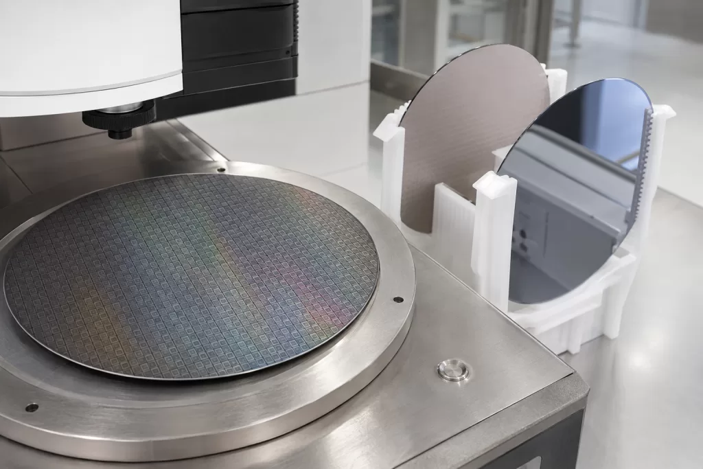
1. Why MEMS Wafer Selection Is Different
In integrated circuits, the silicon wafer mainly provides a platform for transistors and interconnects. In many MEMS devices, the wafer itself becomes part of the mechanical structure.
The silicon may form:
- A pressure-sensing diaphragm
- An accelerometer proof mass
- A gyroscope frame
- A resonating beam
- A microfluidic channel
- An optical mirror
- A cap or cavity
- A through-wafer electrical interconnect
- A thermally isolated membrane
Consequently, wafer properties influence not only process yield but also the final device’s sensitivity, resonance frequency, electrical performance and reliability.
The most important parameters include:
- Crystal orientation
- Orientation accuracy
- Conductivity type and dopant
- Resistivity and resistivity uniformity
- Wafer thickness and thickness tolerance
- Total thickness variation
- Bow and warp
- Front and backside surface finish
- Surface roughness and cleanliness
- Edge profile
- Oxygen and carbon content
- Crystal growth method
- Oxide or epitaxial-layer requirements
2. Crystal Orientation: (100), (110) or (111)?
Silicon is anisotropic. Its mechanical properties and chemical etch rates change with crystallographic direction. The same mask pattern can therefore produce different sidewalls and cavity geometries on wafers with different orientations.
Commercial MEMS wafers are commonly available in (100), (110), (111) and selected off-oriented configurations.
(100) Silicon Wafers
The (100) orientation is the most widely used option for both semiconductor devices and MEMS fabrication.
It offers:
- Broad compatibility with CMOS process lines
- Established oxidation and thin-film processes
- Predictable KOH and TMAH anisotropic etching
- Good availability in SSP, DSP and SOI formats
- Standardized flats, notches and alignment conventions
When a (100) silicon wafer is etched with an alkaline anisotropic etchant, the slow-etching {111} planes form sloped sidewalls. The angle between the wafer surface and these {111} planes is approximately 54.7 degrees.
This behavior is useful for producing:
- V-grooves
- Pyramidal cavities
- Pressure-sensor diaphragms
- Microfluidic channels
- Optical-fiber alignment structures
- Backside openings
KOH etching is highly dependent on silicon crystal orientation, which allows geometries that would be difficult to obtain through isotropic etching. MEMS Exchange
For many standard pressure sensors, microfluidic devices and surface-micromachined structures, (100) is the practical starting point.
(110) Silicon Wafers
The (110) orientation is selected when the process requires particular vertical or nearly vertical {111} sidewalls.
With proper mask alignment, anisotropic wet etching of (110) silicon can expose {111} planes that are perpendicular to the wafer surface. This makes (110) useful for:
- Deep vertical cavities
- High-aspect-ratio wet-etched structures
- Microchannels with specific sidewall geometry
- Mechanical reference structures
- Selected optical and inertial MEMS designs
The mask orientation relative to the crystal axes is especially important. Specifying only “(110) wafer” is insufficient if the layout is not aligned with the required crystallographic direction.
(111) Silicon Wafers
The (111) plane is relatively resistant to common alkaline anisotropic etchants. It often forms the limiting surface during the KOH or TMAH etching of other silicon orientations.
(111) wafers may be selected for:
- Specialized mechanical structures
- Resonators
- Selected piezoresistive sensor designs
- Film-growth requirements
- Bonding structures
- Research devices requiring specific surface symmetry
Because the etch geometry is substantially different from that of (100) silicon, the complete mask and etch design must be qualified specifically for the (111) orientation.
Orientation Accuracy
Orientation tolerance can affect:
- Sidewall angle
- Cavity depth
- V-groove symmetry
- Diaphragm dimensions
- Beam direction
- Resonator performance
- Front-to-back alignment
Demanding bulk-micromachined structures may require tighter orientation accuracy than general-purpose semiconductor wafers. The required tolerance should therefore be stated explicitly rather than relying on the supplier’s standard orientation specification.
3. Resistivity and Conductivity Type
Silicon wafer resistivity is controlled through dopant type and concentration.
Common P-type dopants include:
- Boron
Common N-type dopants include:
- Phosphorus
- Arsenic
- Antimony
MEMS-optimized silicon wafers can cover an extremely broad resistivity range, from highly conductive material to high- and ultra-high-resistivity substrates. As one commercial example, MEMS SSP and DSP wafers are available from below 0.001 Ω·cm to above 7,000 Ω·cm, depending on dopant, orientation and crystal-growth conditions. Okmetic
Low-Resistivity Silicon
Low-resistivity wafers may be selected when the silicon substrate must function as:
- A conductive electrode
- An electrical ground
- Part of an electrostatic actuator
- A low-resistance through-wafer structure
- A conductive cap or package component
Highly doped silicon can reduce substrate resistance and charge accumulation. However, higher dopant concentrations can affect process behavior, junction formation and mechanical loss.
Medium-Resistivity Silicon
Standard-resistivity silicon is commonly used for:
- General MEMS development
- Pressure sensors
- Accelerometers
- Microfluidic structures
- Devices where electrical isolation is provided by oxide or deposited dielectric layers
The acceptable range depends on whether the substrate participates electrically in the device or merely acts as a mechanical support.
High-Resistivity Silicon
High-resistivity silicon is often considered for:
- RF MEMS
- Capacitive sensors
- Resonators
- High-frequency filters
- Silicon interposers
- Low-loss passive devices
- Devices requiring reduced substrate coupling
High resistivity can reduce parasitic current, substrate loss and unwanted capacitive coupling. Commercial high-resistivity wafer platforms are specifically used for BAW, FBAR, XBAR, SAW, RFIC, interposer and quantum-device applications. Okmetic
Bulk Resistivity Is Not the Entire Device Specification
For piezoresistive pressure sensors and accelerometers, the active resistors may be formed by diffusion, ion implantation or an epitaxial layer.
Therefore, specifying the starting wafer resistivity alone does not fully define the sensing element. The designer should also consider:
- Active-layer doping
- Junction depth
- Sheet resistance
- Dopant uniformity
- Temperature coefficient
- Contact resistance
- Crystal direction of the piezoresistors
4. Wafer Thickness and Mechanical Performance
MEMS wafer thickness is not simply a handling parameter. It can directly influence device structure and processing time.
Thickness affects:
- Mechanical stiffness
- Proof-mass volume
- Resonance frequency
- Backside cavity depth
- DRIE etching time
- TSV depth and aspect ratio
- Wafer handling
- Bonding pressure
- Dicing stability
- Final package height
Thicker Silicon Wafers
Thicker wafers provide greater mechanical strength during:
- High-temperature processing
- Backside grinding
- Deep reactive-ion etching
- Film deposition
- Wafer bonding
- Robotic handling
They may also provide more material for proof masses or deep microfluidic structures. However, thicker wafers require longer through-wafer etching and may increase package height.
Thinner Silicon Wafers
Thinner wafers can reduce:
- DRIE processing time
- Through-wafer via depth
- Final sensor thickness
- Device weight
- Material removal requirements
They are more sensitive to:
- Bow and warp
- Edge chipping
- Handling damage
- Film stress
- Vacuum-chuck deformation
- Bonding-induced stress
Temporary carriers or bonded wafer structures may be required when the wafer becomes too thin for standard equipment.
Nominal Thickness Is Not Enough
A MEMS wafer specification should also include:
- Thickness tolerance
- Total thickness variation
- Bow
- Warp
- Site flatness
- Edge exclusion
Low TTV is particularly important for:
- Uniform DRIE depth
- Backside alignment
- Wafer bonding
- Cavity formation
- CMP
- Wafer-level packaging
Commercial 150 and 200 mm MEMS wafers can be manufactured over broad custom thickness ranges, but practical limits depend on diameter, polishing method and handling equipment.
5. Surface Finish and Surface Quality
The required surface finish depends on what will happen on each side of the wafer.
Polished Device Surface
The device side generally requires a polished, semiconductor-grade surface for:
- Photolithography
- Thermal oxidation
- Epitaxy
- Thin-film deposition
- Fine-pattern etching
- Electrical device fabrication
Critical parameters may include:
- Surface roughness
- Haze
- Particles
- Scratches
- Pits
- Crystal-originated defects
- Metallic contamination
- Organic contamination
Wafer Bonding Surface
Fusion bonding and other high-precision bonding processes require tighter surface quality than general lithography.
The bonding surface may require control of:
- Microroughness
- Flatness
- Particles
- Surface chemistry
- Hydrophilic or hydrophobic condition
- Edge profile
- Oxide thickness
- Pre-bond cleaning
A wafer described only as “polished” is not necessarily ready for direct bonding.
Backside Finish
An SSP wafer backside may be:
- Etched
- Lapped
- Polyback coated
- Oxide coated
- Chemically treated
An unpolished backside may be acceptable if it is used only for mechanical support. It may be unsuitable when the process requires backside lithography, infrared alignment, wafer bonding or precise metrology.
6. SSP vs. DSP Silicon Wafers
SSP means single-side polished, while DSP means double-side polished.
The correct choice depends on whether the backside participates in device fabrication, alignment, bonding or packaging.
SSP Silicon Wafers
An SSP wafer has a polished front surface and a non-polished or specially finished backside.
Advantages include:
- Lower cost than DSP wafers
- Suitable front surface for standard lithography
- Good compatibility with surface-micromachined MEMS
- Flexible backside options
- Reduced need to protect two polished surfaces
SSP wafers are commonly suitable for:
- Basic pressure sensors
- Surface MEMS
- Frontside micromachining
- Microfluidic devices
- Micromirrors
- Simple cap wafers
- Research and prototype fabrication
Limitations include:
- Reduced backside optical quality
- More difficult front-to-back alignment
- Limited backside lithography
- Unsuitability for some bonding processes
- Potential backside particle generation
DSP Silicon Wafers
A DSP wafer is polished on both surfaces.
Advantages include:
- Double-sided photolithography
- Accurate front-to-back alignment
- Improved backside inspection
- Better compatibility with wafer bonding
- Controlled thickness uniformity
- Suitability for TSV fabrication
- Lower surface scattering during optical or IR alignment
DSP wafers are commonly used for:
- Advanced accelerometers
- MEMS gyroscopes
- Resonators
- Optical MEMS
- Through-silicon vias
- Bulk micromachining
- Wafer-level caps
- Hermetic sensor packaging
- Double-sided cavities and channels
MEMS wafer suppliers specifically recommend DSP substrates when the process requires double-sided lithography, wafer bonding, backside alignment marks or structures on both surfaces. DSP wafers are also widely used as cap wafers and as platforms for TSV processing. Okmetic
SSP vs. DSP Comparison
| Selection Factor | SSP Wafer | DSP Wafer |
|---|---|---|
| Polished surfaces | Front side only | Front and backside |
| Relative cost | Lower | Higher |
| Frontside lithography | Suitable | Suitable |
| Backside lithography | Limited | Recommended |
| Front-to-back alignment | More difficult | Better |
| Wafer bonding | Suitable for selected processes | Preferred for demanding bonding |
| TSV fabrication | Limited | Commonly selected |
| Optical or IR backside inspection | Limited by backside finish | Better |
| Surface protection during handling | Easier | Both surfaces require protection |
| Typical applications | Surface MEMS, basic sensors, microfluidics | Inertial sensors, resonators, TSV, optical MEMS, cap wafers |
DSP should not be selected automatically. If all device processing occurs on the front side and the backside is only a mechanical support surface, SSP may provide the required performance at lower cost.
7. Wafer Recommendations by MEMS Application
Pressure Sensors
Typical considerations include:
- (100) orientation for predictable anisotropic cavity etching
- SSP for simple frontside structures
- DSP for backside cavity alignment and wafer bonding
- Controlled thickness and TTV for diaphragm uniformity
- Resistivity selected according to piezoresistive or capacitive sensing design
Accelerometers and Gyroscopes
Typical considerations include:
- (100) or (110) orientation depending on etch geometry
- DSP for double-sided alignment and bulk micromachining
- Low bow and warp for lithography and bonding
- Tight thickness control for proof-mass consistency
- SOI for precisely controlled device-layer thickness
Microfluidic Devices
Typical considerations include:
- (100) wafers for wet-etched channels and cavities
- SSP for frontside-only channel fabrication
- DSP for through-wafer ports or double-sided structures
- Bond-ready surfaces for silicon-to-glass or silicon-to-silicon sealing
Optical MEMS and Micromirrors
Typical considerations include:
- Low surface roughness
- Low bow and warp
- DSP for backside alignment and optical inspection
- Tight thickness uniformity
- Crystal orientation matched to mirror-support structures
RF MEMS and Resonators
Typical considerations include:
- High or ultra-high resistivity
- Low oxygen-related thermal donor effects where relevant
- Low substrate loss
- Tight thickness and flatness control
- DSP or SOI depending on device architecture
Cap and Packaging Wafers
Typical considerations include:
- DSP for precise bonding and backside processing
- Low particles and metallic contamination
- Controlled cavities or through-wafer vias
- Tight TTV and flatness
- Compatible surface chemistry for the selected bonding method
8. When to Consider SOI Instead of Bulk Silicon
SSP and DSP describe surface finishing, but they do not define the internal wafer structure.
When the MEMS device requires a precisely controlled structural thickness, a silicon-on-insulator wafer may be more suitable than bulk silicon.
SOI provides:
- A defined silicon device layer
- A buried oxide etch stop
- Electrical isolation
- Controlled membrane or beam thickness
- Simplified release processing
- Reduced variation in mechanical structures
The buried oxide can function as an insulator, etch stop or sacrificial layer, while the handle wafer provides mechanical support. Okmetic
SOI is commonly used for advanced inertial sensors, resonators, microphones and devices where mechanical thickness directly controls performance.
9. Silicon Wafer Specification Checklist
A complete MEMS silicon wafer inquiry should include:
- Application or sensor type
- Wafer diameter
- Crystal orientation
- Orientation tolerance
- Primary flat or notch direction
- P-type or N-type
- Dopant species
- Target resistivity range
- Resistivity uniformity
- Crystal growth method
- Oxygen concentration if critical
- Nominal thickness
- Thickness tolerance
- Total thickness variation
- Bow and warp
- SSP or DSP
- Backside finish for SSP
- Frontside surface roughness
- Backside surface roughness for DSP
- Particle and metallic contamination limits
- Edge profile
- Edge exclusion
- Thermal oxide requirements
- Epitaxial-layer requirements
- Alignment-mark requirements
- Laser-marking restrictions
- Packaging and cleanliness requirements
- Intended etching and bonding processes
Providing the application and process flow helps the supplier determine whether a standard wafer is sufficient or a customized MEMS wafer is required.
10. Common Selection Mistakes
Specifying Orientation Without Mask Direction
The wafer orientation and mask alignment must be considered together for anisotropic wet etching. Incorrect alignment can change sidewall geometry and final feature dimensions.
Selecting Resistivity Without Considering the Device Circuit
The correct resistivity depends on whether the substrate acts as a conductor, insulator, electrode, mechanical support or RF platform.
Specifying Only Nominal Thickness
TTV, bow and warp may be more important than nominal thickness for bonding, DRIE and double-sided lithography.
Choosing DSP Only Because It Appears Higher Grade
DSP offers important process advantages, but it adds cost and handling requirements. SSP is often sufficient for frontside-only MEMS devices.
Treating Every Polished Surface as Bond-Ready
Surface roughness, particles, flatness and surface chemistry must be matched to the actual bonding method.
Ignoring SOI as an Alternative
When the device requires a precise beam, membrane or proof-mass thickness, SOI may provide better control than timed etching of a bulk wafer.
Conclusion
Selecting a silicon wafer for MEMS and sensor fabrication requires much more than choosing a diameter and thickness.
Crystal orientation determines anisotropic etching behavior and mechanical geometry. Resistivity affects conductivity, isolation, parasitic coupling and RF loss. Thickness controls stiffness, proof mass, etch time and handling stability. Surface finish determines whether the wafer can support backside lithography, optical alignment, TSV fabrication and wafer bonding.
SSP wafers remain a cost-effective choice for frontside processing and many conventional sensors. DSP wafers are preferred when both surfaces participate in lithography, alignment, micromachining or bonding. For devices requiring precisely defined structural layers, SOI may offer a more controllable platform than bulk silicon.
The best substrate is the wafer whose crystal, electrical, mechanical and surface specifications are designed around the complete MEMS process flow.