
Not all defects in a silicon carbide wafer have the same impact.
Some imperfections may primarily affect surface appearance. Others can reduce device yield immediately.
A particularly important class of defects is more difficult to manage because the device may initially appear normal but degrade during operation.
One of the best-known examples in 4H-SiC is the relationship between basal plane dislocations (BPDs) and stacking-fault expansion.
This issue has been studied for many years, yet research published in 2026 continues to reveal new details about where expandable stacking faults originate and how different dislocation structures evolve.
That continued research is significant because SiC power electronics are increasingly being used in applications expected to operate for many years under high current, high voltage and elevated temperature.
In these applications, long-term defect stability matters as much as initial electrical performance.
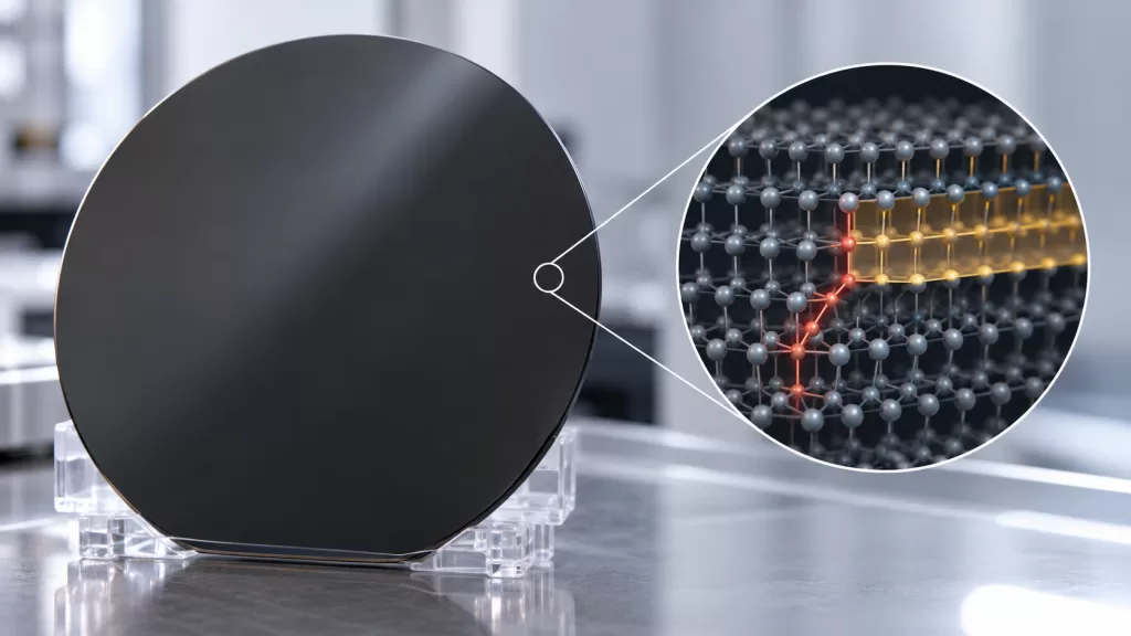
What Is a Basal Plane Dislocation?
4H-SiC is a crystalline material consisting of periodically arranged silicon and carbon atoms.
A perfect crystal would repeat this atomic structure continuously.
Real crystals contain imperfections.
A dislocation is a line defect representing a disruption in the ideal atomic arrangement.
A basal plane dislocation is located on the basal crystallographic plane of the SiC crystal.
BPDs may originate during bulk crystal growth and can interact with the subsequent epitaxial layer.
Depending on growth conditions, some BPDs may convert into other dislocation types during epitaxy, while others can propagate into the epilayer.
This distinction is important because BPDs in the active epitaxial region can become sources for stacking faults under certain carrier-injection conditions.
From BPD to Stacking Fault
One reliability mechanism associated with SiC bipolar operation is the expansion of a Shockley-type stacking fault.
A stacking fault is a planar interruption in the normal atomic stacking sequence of the crystal.
Under carrier injection, energy associated with electron-hole recombination can promote expansion of a fault from certain dislocations.
As the stacking fault expands through the active area of the device, its electrical characteristics may change.
Historically, this phenomenon has been associated particularly with bipolar SiC devices such as PiN diodes.
However, modern SiC MOSFET structures may also include a body diode that experiences bipolar current under certain operating conditions.
Therefore, understanding expandable defects remains relevant to SiC power electronics.
2026 Research Is Showing That the Origins Are More Complex
The traditional explanation often focuses on BPDs propagating from the substrate into the epitaxial layer.
Recent research indicates that the defect picture can be more complicated.
A January 2026 study used X-ray topography and photoluminescence imaging before and after ultraviolet-induced stacking-fault expansion to investigate the origins of single Shockley stacking faults in 4H-SiC epitaxial wafers.
The researchers identified not only known substrate-related and propagated BPD origins, but also origins associated with surface regions and threading mixed dislocations.
Further research published in August 2026 identified a threading mixed dislocation associated with the origin of a single Shockley-type stacking fault and examined how basal-plane components could be released from a more complex dislocation structure.
These results matter because defect reduction cannot rely only on counting one simple defect category.
The structure, orientation and evolution of the defect can determine whether it becomes electrically significant.
Different BPD Structures May Behave Differently
Another 2026 study investigated different types of basal plane dislocations in 4H-SiC and their evolution.
The work used optical and diffraction-related characterization to distinguish BPD structures and examine their behavior during epitaxial growth.
This reflects a broader change in SiC defect engineering.
The industry is moving from asking:
“How many dislocations are present?”
toward asking:
“What type of dislocations are present, where are they located and how will they behave during epitaxy and device operation?”
Two wafers with a similar total dislocation count may therefore behave differently if the defect populations are different.
Why Epitaxy Is Critical
The substrate is only the starting point.
Power-device performance depends strongly on what happens when the epitaxial layer is grown.
During homoepitaxy, substrate defects can propagate, transform or terminate.
A well-controlled epitaxial process can convert some BPDs into threading edge dislocations, which are generally less problematic for bipolar degradation than BPDs remaining in the active layer.
However, the conversion is not perfect.
Surface preparation, off-axis orientation, growth temperature, C/Si ratio, growth rate and reactor conditions can all influence step-flow growth and defect evolution.
Research published in 2026 continues to examine how surface micro-defects disturb step-flow growth on 4° off-axis 4H-SiC substrates. Such disturbances can contribute to step bunching and other epitaxial surface abnormalities.
This demonstrates why substrate polishing and epitaxial defect control cannot be treated as completely separate issues.
Why 4° Off-Axis SiC Is Common
Commercial 4H-SiC power substrates are often cut several degrees away from the exact (0001) basal plane.
A 4° off-axis orientation toward the appropriate crystallographic direction is widely used.
The slight misorientation creates atomic steps across the wafer surface.
During homoepitaxy, incoming atoms can attach at these steps, promoting step-flow growth and helping preserve the desired 4H-SiC polytype.
However, this also means that polishing damage, pits and local step irregularities can influence subsequent growth.
If a surface defect interrupts the regular step structure, localized step bunching or other morphology problems may occur.
Consequently, crystal orientation, polishing quality and epitaxial parameters must be considered together.
How Are BPDs and Stacking Faults Detected?
No single inspection technique provides all the information required for SiC defect analysis.
X-ray topography is particularly valuable because it can visualize crystallographic strain fields and dislocation structures over relatively large wafer areas without destroying the wafer.
Photoluminescence imaging can reveal optically active defects and is widely used for epitaxial-wafer defect characterization.
UV irradiation can also be used experimentally to stimulate stacking-fault expansion, helping researchers identify potentially expandable defect origins.
Other techniques may include molten KOH etching, optical microscopy, scanning electron microscopy, cathodoluminescence and transmission electron microscopy.
The correct inspection method depends on whether the objective is production screening, root-cause analysis or atomic-scale defect identification.
Why Device Size Changes the Defect Problem
Defect density is usually expressed per unit area.
This means die size matters.
If a wafer contains a fixed defect density, a larger die covers more wafer area and therefore has a greater statistical probability of intersecting a critical defect.
This becomes particularly relevant as SiC devices move toward higher current and higher voltage ratings.
Larger die and more demanding blocking structures increase the economic value of low-defect starting material.
A substrate improvement that appears modest when expressed as defects per square centimeter can produce a much larger improvement in usable die yield for large-area devices.
Initial Yield Is Not the Same as Long-Term Reliability
One of the most important lessons from BPD-related degradation is that initial electrical testing cannot detect every future reliability risk.
A device may pass its initial voltage, leakage and on-resistance specifications.
If an expandable defect later changes under prolonged current injection, the electrical behavior of the device may drift.
This distinction is especially important for electric vehicles, renewable-energy inverters, industrial drives and grid equipment, where devices may operate for many thousands of hours.
Material qualification therefore needs to consider both immediate defect-related yield and potential long-term defect evolution.
What SiC Wafer Buyers Should Ask
Purchasing a SiC wafer based only on diameter, thickness and surface roughness provides an incomplete picture for device-grade applications.
For demanding development and production programs, buyers may also need information about micropipes, threading screw dislocations, threading edge dislocations, basal plane dislocations, stacking faults and epitaxial killer defects.
It is equally important to understand the measurement method.
A defect specification measured by X-ray topography should not automatically be compared with a value obtained using photoluminescence or etch-pit inspection without understanding what each method detects.
For meaningful supplier comparison, both the numerical specification and the inspection methodology matter.
Defect Engineering Is Becoming Part of Device Engineering
As SiC substrate quality improves, the remaining defects become increasingly important rather than less important.
Once very large defects such as micropipes are reduced to extremely low levels, attention shifts to smaller and more complex crystallographic defects.
The 2026 research on BPDs, threading mixed dislocations and stacking-fault origins reflects this transition.
The next generation of SiC power devices will not depend only on lower on-resistance and larger wafer diameter.
It will also depend on controlling defects that may influence performance thousands of hours after the device leaves the factory.
For SiC substrate and epitaxial wafer suppliers, this makes defect characterization much more than a quality-control task.
It is becoming a fundamental part of long-term device reliability engineering.