Sapphire wafers, composed of crystalline aluminum oxide, have garnered significant attention across multiple industries due to their exceptional properties. This abstract aims to provide an extensive overview of sapphire wafers, exploring their diverse applications, manufacturing processes, and performance characteristics.
Initially used primarily in the semiconductor industry as substrates for gallium nitride (GaN) epitaxy, sapphire wafers have since expanded their utility to encompass a broad spectrum of applications. Their high thermal conductivity, optical transparency spanning from ultraviolet to infrared wavelengths, and remarkable hardness render them indispensable in fields ranging from optoelectronics and photonics to aerospace and defense.
Manufacturing processes for sapphire wafers vary depending on the desired specifications and applications. Techniques such as Verneuil, Czochralski, and heat exchange methods are employed to grow single-crystal sapphire ingots, which are subsequently sliced and polished into wafers of various sizes and thicknesses. Post-growth treatments, including annealing and chemical-mechanical polishing, further enhance the crystalline quality and surface finish of the wafers.
In terms of performance, sapphire wafers exhibit outstanding mechanical robustness, with hardness second only to diamond, making them resistant to scratches and wear. Their thermal stability and resistance to chemical corrosion enable their deployment in harsh environments and high-temperature applications, including aerospace components and high-power electronics.
The optical properties of sapphire wafers, characterized by high transparency and minimal birefringence, facilitate their use in optical windows, lenses, and substrates for lasers and sensors. Their broadband transmission capabilities and low absorption coefficients make them particularly well-suited for ultraviolet, visible, and infrared optical systems.
In conclusion, sapphire wafers represent a versatile material platform with unparalleled properties, driving innovation across diverse sectors. Continued research and development efforts aimed at optimizing manufacturing processes and exploring novel applications are poised to further elevate the significance of sapphire wafers in advancing technology and scientific discovery.
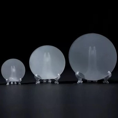
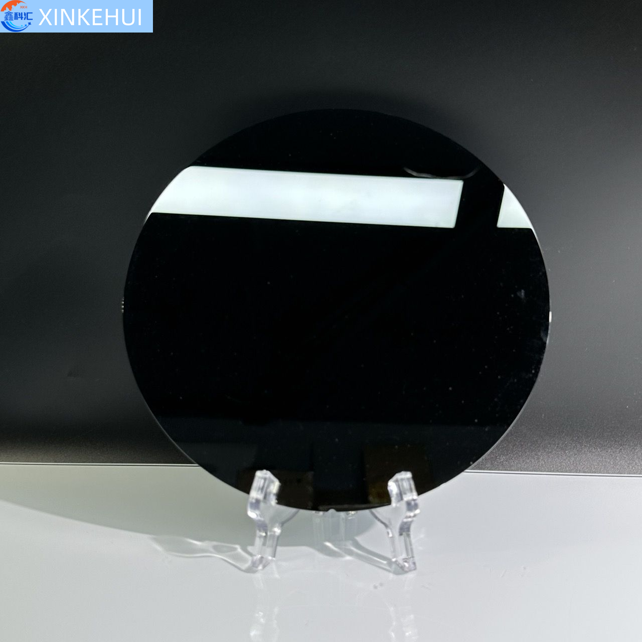
Sapphire Wafer‘s feature
High Hardness: Sapphire wafers possess remarkable hardness, second only to diamond, making them highly resistant to scratches and wear. This feature ensures their durability and longevity in demanding environments.
Excellent Optical Transparency: Sapphire wafers exhibit high optical transparency across a broad spectrum, ranging from ultraviolet (UV) to infrared (IR) wavelengths. This property makes them suitable for optical applications requiring superior light transmission.
High Thermal Conductivity: With a thermal conductivity comparable to that of aluminum nitride and beryllium oxide, sapphire wafers efficiently dissipate heat generated by electronic or optical components. This feature is crucial for thermal management in high-power devices.
Chemical Inertness: Sapphire wafers are chemically inert and resistant to most acids and alkalis, ensuring their stability in corrosive environments. This property makes them suitable for use in chemical processing and harsh industrial settings.
Crystalline Structure: As single-crystal substrates, sapphire wafers exhibit a uniform and well-defined crystalline structure, which is essential for epitaxial growth processes in semiconductor manufacturing. This feature enables precise control over device performance and characteristics.
Wide Bandgap: Sapphire wafers have a wide bandgap, making them optically transparent and electrically insulating. This property is advantageous for applications requiring isolation or protection from electrical currents and electromagnetic interference.
Biocompatibility: Sapphire wafers are biocompatible, making them suitable for use in biomedical devices and implants. Their inert nature and compatibility with biological tissues minimize adverse reactions and ensure compatibility with the human body.
Mechanical Strength: Apart from hardness, sapphire wafers also exhibit high mechanical strength, allowing them to withstand mechanical stresses and mechanical loads without deformation or fracture.
Sapphire wafers’s specifications
Orientation
R-plane, C-plane, A-plane, M-plane or a specified orientation
≤10µm for 2 inches, ≤15µm for 3 inches, ≤20µm for 4 inches, ≤25µm for 6 inches
BOW
≤10µm for 2 inches, ≤15µm for 3 inches, ≤20µm for 4 inches, ≤25µm for 6 inches
Front Surface
Epi-Polished (Ra< 0.3nm for C-plane, 0.5nm for other orientations)
Back Surface
Fine ground (Ra=0.6μm~1.4μm) or Epi-polished
Packaging
Packaged in a class 1000 clean room environment
Sapphire wafers’ applications
Semiconductor Manufacturing: Sapphire wafers serve as substrates for the epitaxial growth of gallium nitride (GaN) and other semiconductor materials. They are used in the production of high-brightness LEDs (HB-LEDs), laser diodes, radio-frequency integrated circuits (RFICs), and power electronics. The high thermal conductivity and excellent electrical insulation of sapphire wafers make them ideal for such applications.
Optoelectronics and Photonics: Due to their high optical transparency and wide bandgap, sapphire wafers are utilized in various optical components, including windows, lenses, prisms, and optical filters. They are employed in ultraviolet (UV), visible, and infrared (IR) optical systems, such as cameras, sensors, laser systems, and spectrometers.
Aerospace and Defense: Sapphire wafers are used in aerospace and defense applications where durability, reliability, and resistance to harsh environments are critical. They are employed in optical windows for aircraft and spacecraft, protective covers for sensors and detectors, and components for high-performance missiles and surveillance systems.
High-Temperature and Harsh Environments: The thermal stability and chemical inertness of sapphire wafers make them suitable for use in high-temperature and corrosive environments. They are utilized in furnace windows, combustion chambers, chemical processing equipment, and sensors for industrial applications.
MEMS (Micro-Electro-Mechanical Systems): Sapphire wafers are used in MEMS devices for their excellent mechanical properties, including high hardness, stiffness, and resistance to wear. They are employed in accelerometers, gyroscopes, pressure sensors, and resonators for automotive, consumer electronics, and medical applications.
Biomedical Devices: The biocompatibility of sapphire wafers makes them suitable for biomedical applications, including implants, surgical tools, and diagnostic instruments. They are utilized in dental implants, artificial joints, and sensors for medical monitoring and diagnostic devices.
Consumer Electronics: Sapphire wafers are increasingly used in consumer electronics, particularly in smartphones and smartwatches, where they serve as scratch-resistant covers for camera lenses, touchscreens, and display panels.
Lasers and Fiber Optics: Sapphire wafers are utilized in laser systems and fiber optic communication networks. Their high optical quality and resistance to optical damage make them suitable for laser cavities, optical waveguides, and fiber optic connectors, improving the performance and reliability of laser-based systems.
Scientific Instruments: Sapphire wafers are employed in scientific instruments and research equipment due to their exceptional optical and mechanical properties. They are used in spectroscopy, microscopy, and laboratory instrumentation, where precision, stability, and durability are essential for accurate measurements and observations.
Water Purification and Filtration: Sapphire wafers are utilized in water purification and filtration systems for their chemical inertness and resistance to corrosion. They are incorporated into membranes and filters for removing impurities and contaminants from water, ensuring clean and safe drinking water in residential, commercial, and industrial settings.
Watch Crystals: Sapphire wafers are commonly used as watch crystals in high-end timepieces. Their scratch-resistant surface and optical clarity make them ideal for protecting watch dials and movements, ensuring longevity and precision in mechanical and quartz watches.
Medical Imaging: Sapphire wafers are employed in medical imaging devices, such as endoscopes and optical coherence tomography (OCT) systems. Their optical transparency and biocompatibility enable high-resolution imaging of biological tissues and structures, aiding in diagnosis and medical treatment.
Solar Cells and Photovoltaics: Sapphire wafers are used in solar cells and photovoltaic modules as substrates for thin-film deposition and as protective covers for photovoltaic cells. Their high optical transparency and durability enhance the efficiency and reliability of solar energy conversion systems.
Artificial Intelligence and Quantum Computing: Sapphire wafers are being explored for use in artificial intelligence hardware accelerators and quantum computing systems. Their high thermal conductivity and electrical insulation properties are advantageous for dissipating heat and minimizing interference in advanced computing architectures.
Sapphire wafers’ showcase
Production process
The production process of sapphire wafers using the Kyropoulos (KY) method involves several detailed steps. Here’s a comprehensive overview:
Raw Material Selection: High-purity aluminum oxide (Al2O3) is selected as the raw material for sapphire wafer production. The quality of the raw material is crucial for achieving high-quality wafers with minimal defects.
Crystal Growth: The Kyropoulos method involves the growth of single-crystal sapphire ingots from the melt. The process begins by melting the alumina feedstock in a crucible made of refractory material, typically molybdenum or platinum. A seed crystal, oriented along the desired crystallographic axis, is slowly lowered into the melt. As the crucible is slowly cooled, sapphire crystallizes on the seed crystal, forming a cylindrical ingot.
Controlled Cooling: The cooling rate during crystal growth is carefully controlled to minimize thermal stresses and ensure uniform crystal quality. Slow and controlled cooling helps to reduce dislocations and other crystal defects that can degrade wafer performance.
Ingot Extraction: Once the crystal growth is complete, the sapphire ingot is extracted from the crucible. The ingot is typically annealed to relieve internal stresses and improve crystal uniformity.
Slicing: The sapphire ingot is precision-sliced into thin wafers using diamond saws or wire saws. The wafers are cut perpendicular to the crystallographic c-axis to optimize their optical and mechanical properties.
Grinding and Polishing: The sliced wafers undergo grinding and polishing processes to achieve the desired thickness and surface finish. Grinding removes excess material and rough surface imperfections, while polishing produces a smooth and optically flat surface.
Cleaning and Inspection: The polished wafers are thoroughly cleaned to remove any contaminants or residues. They undergo rigorous inspection to ensure dimensional accuracy, surface quality, and absence of defects such as cracks, scratches, or impurities.
Final Quality Control: Each sapphire wafer undergoes final quality control checks to verify its optical and mechanical properties. Advanced testing methods, including optical microscopy, X-ray diffraction, and spectrophotometry, may be employed to assess crystal orientation, transparency, and other key parameters.
Packaging and Storage: The finished sapphire wafers are carefully packaged to protect them from damage during transportation and storage. They are typically stored in clean and controlled environments to maintain their quality and performance.
Optional Coating: Depending on the intended application, sapphire wafers may undergo additional processes such as surface coating or doping to modify their optical or electrical properties.
By following these detailed steps, manufacturers can produce high-quality sapphire wafers suitable for a wide range of applications in industries such as electronics, optics, aerospace, and more.
Our factory
XINKEHUI is specializing in the research, production, processing, and sales of Semiconductor substrates and opta:rystal materials. Our products are widely used in Semiconductor, and optical electronics, consumer electfonics, themilitary industry, as well as the fields of laser and optical communication.
The XINKEHUI rely on Hiubel ingling Technology itd. and our main produced products include sapphire optical windows, Colored Sapphire, sapphilre optical components, equipment instrument accessories, moble phone lens covers, sapphire bearings, specialshaped non-standard parts, and special ceramics,ithlum tantalate, slicon carbide, quartz, as well as various semiconductor crystal materials and wafers.
We have an experienced engineering team, management expertise, precision processing equipment, and testing instruments,providing us with extremely strong capablities in processing non-standard products. We can research, develop, and design variousnew products according to customer needs. The company will adhere to the principle of “customer-centered, quality-based” andstrive to become a top-tier high-tech enterprise in the field of optoelectronic materials.
Our service
At XINKEHUI, we take pride in offering unparalleled sapphire wafer customization services tailored to meet the unique needs of our clients. With a meticulous attention to detail and a commitment to excellence, we provide a comprehensive range of customization options, coupled with efficient FedEx shipping and impeccable after-sales support.
Customization Excellence:
Our company specializes in every stage of the sapphire wafer production process, ensuring that each wafer meets the exact specifications and requirements of our customers. Whether it’s the selection of high-purity raw materials, precision slicing and polishing, or advanced surface coating techniques, we leverage cutting-edge technology and expertise to deliver customized solutions that exceed expectations.
From precise control over crystal orientation and thickness to tailored surface finishes and coatings, we offer a wide range of customization options to suit diverse applications across industries such as semiconductor manufacturing, optoelectronics, aerospace, and more. Our experienced team works closely with clients to understand their specific needs and provide personalized recommendations to achieve optimal results.
Efficient FedEx Shipping:
At XINKEHUI, we understand the importance of timely delivery and reliable logistics. That’s why we partner with FedEx, a global leader in shipping and logistics, to ensure fast and efficient transportation of our customized sapphire wafers to destinations worldwide. With FedEx’s extensive network and track record of reliability, our customers can have peace of mind knowing that their orders will arrive on time and in pristine condition.
Whether it’s a small batch of prototype wafers or a large-scale production order, we prioritize efficiency and reliability in every step of the shipping process. From order processing and packaging to tracking and delivery, our integrated approach ensures seamless logistics management and timely arrival of our products to our customers’ doorsteps.
Superior After-Sales Support:
At XINKEHUI, our commitment to customer satisfaction extends beyond the point of sale. We stand behind the quality and performance of our customized sapphire wafers and strive to provide superior after-sales support to address any questions, concerns, or issues that may arise.
Our dedicated customer support team is available to assist clients with technical inquiries, product troubleshooting, and warranty claims, ensuring a positive and hassle-free experience throughout the entire lifecycle of our products. Whether it’s providing expert guidance on wafer handling and integration or offering timely solutions to resolve any issues, we are committed to fostering long-term partnerships with our customers based on trust, reliability, and mutual success.
In conclusion, at XINKEHUI, we are dedicated to delivering excellence in sapphire wafer customization services, supported by efficient FedEx shipping and superior after-sales support. With our unwavering commitment to quality, reliability, and customer satisfaction, we strive to be the preferred partner for businesses and organizations seeking customized sapphire solutions for their cutting-edge applications.
Q&A
What are sapphire wafers used for?
Sapphire wafers and substrates find extensive applications in numerous high-tech industries. They are fundamental in producing semiconductor devices, where their thermal stability and electrical insulation properties offer substantial advantages.
Is sapphire wafer better than silicon?
Compared to silicon, it has a thermal mismatch, lattice mismatch, and poor electrical conductivity. For these reasons, it is best not to use sapphire in LEDs. Another disadvantage is its incompatibility. As silicon has failed to replace sapphire as a substrate, the manufacturers use silicon instead.
Why sapphire is used as substrate?
Sapphire has exceptional electrical insulation, transparency, good thermal conductivity, and high rigidity properties. Hence it is an ideal material for substrates and is used in LED and microelectronic circuits, ultra-high-speed integrated circuits.
High Thermal Conductivity: Sapphire possesses excellent thermal conductivity, second only to diamond among insulating materials. This property allows it to efficiently dissipate heat generated by electronic devices, making it ideal for high-power applications where thermal management is critical.
Electrical Insulation: Sapphire is an excellent electrical insulator, meaning it does not conduct electricity. This property is advantageous for isolating electronic components and preventing electrical leakage or short circuits in devices such as transistors, diodes, and integrated circuits.
Chemical Stability: Sapphire is highly resistant to chemical corrosion, even in harsh environments or when exposed to corrosive substances. This makes it suitable for use in semiconductor processing, where exposure to chemicals is common during fabrication processes.