
Zprávy
Proč jsou 300mm křemíkové pláty důležité pro výrobu pokročilých polovodičů?
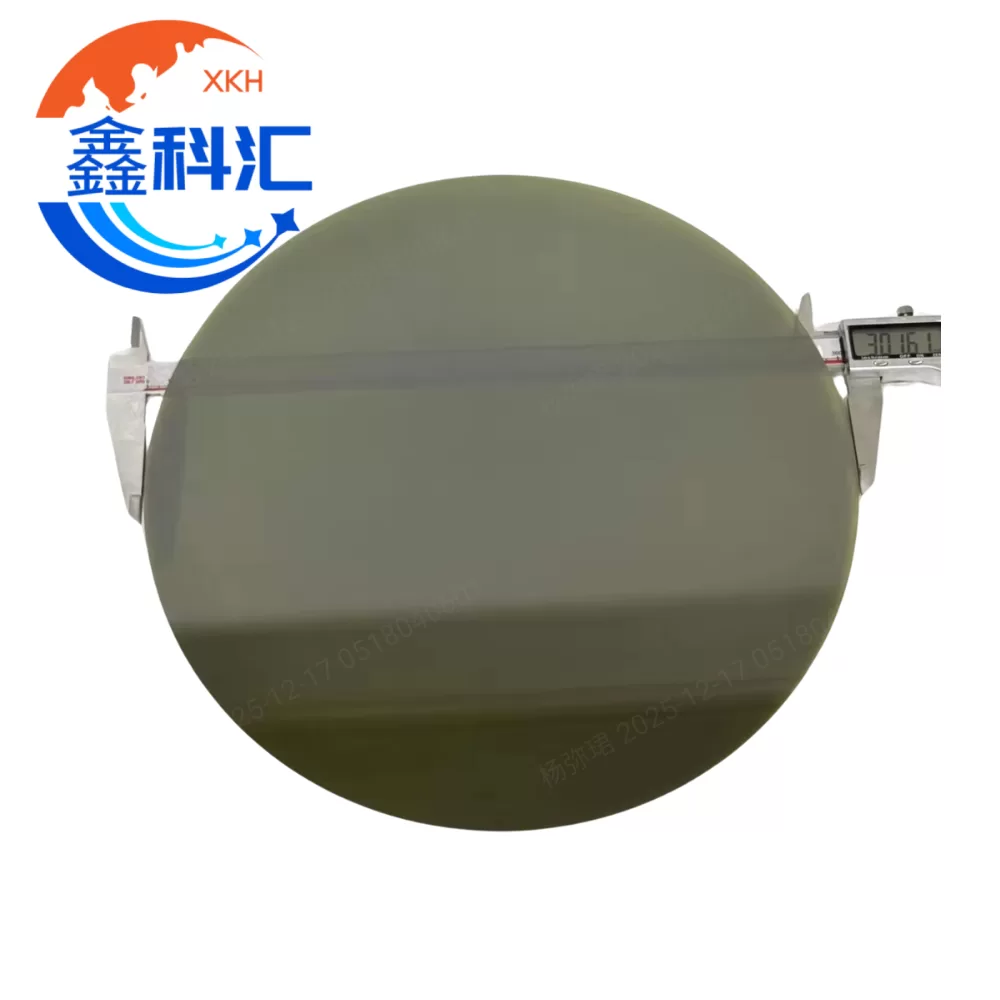
The transition from 200mm to 300mm silicon wafers represents one of the most significant structural upgrades in the semiconductor manufacturing ecosystem. Beyond a simple increase