
CZ-Si Wafers’ abstract
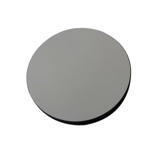
CZ-Si (Czochralski Silicon) wafers play a critical role in the semiconductor industry, serving as the foundation for the fabrication of various electronic devices. These wafers are produced using the Czochralski method, a process that enables the growth of high-purity single-crystal silicon ingots. CZ-Si wafers possess distinctive characteristics that make them highly suitable for a wide range of applications in integrated circuit manufacturing and other semiconductor industries.
One of the key features of CZ-Si wafers is their high purity. The Czochralski method allows for the precise control of impurities during crystal growth, resulting in silicon wafers with extremely low levels of contamination. This high purity is essential for ensuring the reliable performance and longevity of semiconductor devices, particularly in advanced electronic applications where even trace impurities can impact device performance.
Another characteristic of it is their excellent crystal quality. The single-crystal structure of CZ-Si wafers provides uniform electrical properties throughout the wafer, making them ideal substrates for the fabrication of integrated circuits and other electronic components. This uniformity is crucial for achieving consistent device performance and yields in semiconductor manufacturing processes.
CZ-Si wafers are utilized in various stages of the integrated circuit manufacturing process. During wafer fabrication, CZ-Si wafers serve as the starting material for the deposition, patterning, and etching of semiconductor layers to create electronic devices. The high purity and crystal quality of CZ-Si wafers ensure the precise control of device dimensions and electrical properties, leading to the production of high-performance integrated circuits.
In addition to integrated circuit manufacturing, it find applications in other semiconductor industries such as optoelectronics, photovoltaics, and MEMS (Microelectromechanical Systems). In optoelectronic applications, they are used as substrates for the fabrication of photonic devices such as LEDs (Light-Emitting Diodes) and laser diodes. In photovoltaic applications, they are employed in the production of solar cells for renewable energy generation. In MEMS applications, CZ-Si wafers serve as the foundation for the fabrication of microsensors and actuators used in various electronic systems.
Overall, CZ-Si wafers are indispensable materials in the semiconductor industry, supporting the advancement of electronic technology across a wide range of applications. Their high purity, excellent crystal quality, and versatility make them essential components in the production of integrated circuits and other semiconductor devices, driving innovation and progress in electronics, optoelectronics, and renewable energy.
CZ-Si Wafers’ applications
Applications in Integrated Circuit Manufacturing:
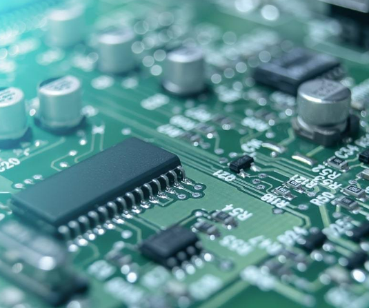
In the realm of integrated circuit manufacturing, CZ-Si wafers serve as the cornerstone upon which intricate electronic devices are meticulously crafted. These wafers embark on a journey of transformation, undergoing a series of precise processes to actualize the blueprint of semiconductor layers, thus giving birth to complex electronic components. Through epitaxial growth, ion implantation, and lithography, they intricately define the structural intricacies and electrical characteristics of these devices. With CZ-Si wafers as their canvas, manufacturers sculpt high-performance integrated circuits with unparalleled precision, facilitating significant strides in semiconductor technology.
Applications in Optoelectronics:
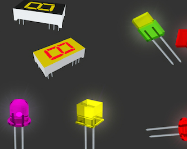
CZ-Si wafers emerge as pivotal substrates in the intricate realm of optoelectronics, where light and electricity intertwine to power cutting-edge technologies. The pristine crystal quality and uniformity of CZ-Si wafers render them ideal canvases for the cultivation of epitaxial layers boasting meticulously controlled optical properties. Within LED manufacturing, they form the very foundation upon which semiconductor materials are deposited, culminating in the emission of radiant light upon forward biasing. Similarly, CZ-Si wafers serve as the bedrock for laser diodes, facilitating the generation of coherent light waves for a myriad of applications spanning telecommunications, optical storage, and medical devices. Furthermore, CZ-Si wafers find themselves at the heart of photodetector fabrication, enabling the detection of light across diverse domains such as imaging, sensing, and communication.

Applications in Photovoltaics:
In the quest for sustainable energy solutions, they emerge as indispensable protagonists in the realm of photovoltaics, driving the transition towards renewable energy sources. As the backbone of solar cell production, CZ-Si wafers play a pivotal role in harnessing the boundless potential of sunlight and transforming it into electricity through the magic of the photovoltaic effect. With their unmatched purity and crystal quality, CZ-Si wafers ensure the efficient capture and conversion of solar energy, yielding high-performance solar panels boasting exceptional power output and reliability. Whether in the realm of crystalline silicon or thin-film solar cell technologies, CZ-Si wafers catalyze the evolution of the solar energy industry, paving the way towards a brighter, sustainable future.

In microelectronics, they serve as the substrate for the fabrication of microelectromechanical systems (MEMS) and integrated circuits. MEMS devices, including sensors, actuators, and microfluidic systems, are manufactured using processes such as surface micromachining, bulk micromachining, and deposition of thin-film materials. CZ-Si wafers provide a stable and reliable platform for fabricating MEMS devices with precise mechanical and electrical properties. Additionally, they are used in the production of integrated circuits for various applications, including consumer electronics, automotive systems, and medical devices.
CZ-Si (Czochralski silicon) wafers stand as foundational materials within the realm of semiconductor manufacturing and its related industries. Their significance lies in their remarkable properties—high purity, exceptional crystal quality, and uniform electrical characteristics—rendering them indispensable components in various technological applications. As electronic advancements surge forward, the demand for CZ-Si wafers is poised to escalate, fueling innovation, catalyzing progress in semiconductor technology, and spearheading the development of novel applications across diverse sectors.
Semiconductor technology underpins the modern digital age, serving as the bedrock for numerous electronic devices. CZ-Si wafers, with their pristine quality, play a pivotal role in the production of integrated circuits (ICs), the building blocks of electronic devices. ICs, also known as microchips, are omnipresent in everyday gadgets, from smartphones and computers to household appliances and automobiles. The relentless pursuit of smaller, faster, and more efficient electronic devices propels the demand for them, as they facilitate the fabrication of intricate circuitry with nanoscale precision.
Moreover, optoelectronic devices leverage CZ-Si wafers for their optical and electronic functionalities. These devices include light-emitting diodes (LEDs), photodetectors, and optical sensors, which find applications in displays, lighting systems, communication networks, and medical devices. CZ-Si wafers, with their superior material properties, enable the precise control of light emission and detection, thus enhancing the performance and reliability of optoelectronic systems.
In the realm of renewable energy, CZ-Si wafers serve as the cornerstone for photovoltaic (PV) cells, which convert sunlight into electricity. With the global push towards sustainable energy solutions, the demand for solar panels continues to escalate. CZ-Si wafers, renowned for their exceptional efficiency and durability, contribute to the proliferation of solar energy systems worldwide. The scalability and cost-effectiveness of CZ-Si-based PV technology make solar power an increasingly viable alternative to conventional energy sources, driving the transition towards a greener future.
Furthermore, CZ-Si wafers play a crucial role in the fabrication of Micro-Electro-Mechanical Systems (MEMS), miniature devices that integrate mechanical and electrical components on a single chip. MEMS devices encompass a diverse range of applications, including inertial sensors, microphones, accelerometers, and pressure sensors. These miniaturized devices find utility in consumer electronics, automotive systems, healthcare devices, and industrial automation, among other domains. CZ-Si wafers enable the precise fabrication of MEMS structures with high aspect ratios and intricate geometries, enabling the realization of compact, high-performance devices.
As the demand for CZ-Si wafers continues to soar, the semiconductor industry is witnessing a paradigm shift towards advanced manufacturing processes and materials. Innovations such as silicon-on-insulator (SOI) technology, epitaxial growth techniques, and advanced lithography methods are enhancing the performance and functionality of semiconductor devices. Additionally, research efforts are underway to explore alternative materials and substrates, including gallium nitride (GaN), silicon carbide (SiC), and flexible substrates, to address the evolving needs of diverse applications.
The proliferation of CZ-Si wafers and associated semiconductor technologies is poised to revolutionize various sectors, including telecommunications, healthcare, transportation, and entertainment. In telecommunications, the deployment of high-speed data networks, such as 5G, relies on advanced semiconductor devices for signal processing and data transmission. In healthcare, semiconductor-based sensors and imaging devices enable precise diagnosis, monitoring, and treatment of medical conditions.
In transportation, semiconductor technology powers autonomous vehicles, electric vehicles, and advanced driver assistance systems (ADAS), enhancing safety and efficiency on the roads. In entertainment, immersive technologies like virtual reality (VR) and augmented reality (AR) leverage semiconductor components for immersive user experiences.
The synergy between CZ-Si wafers and semiconductor technology fuels a virtuous cycle of innovation, driving continuous improvements in performance, power efficiency, and cost-effectiveness. As the semiconductor industry embraces new materials, processes, and design methodologies, CZ-Si wafers will remain at the forefront, enabling the realization of next-generation electronic devices and ushering in an era of unprecedented technological progress. In essence, CZ-Si wafers epitomize the transformative power of materials science and semiconductor engineering, shaping the trajectory of human civilization in the digital age and beyond.
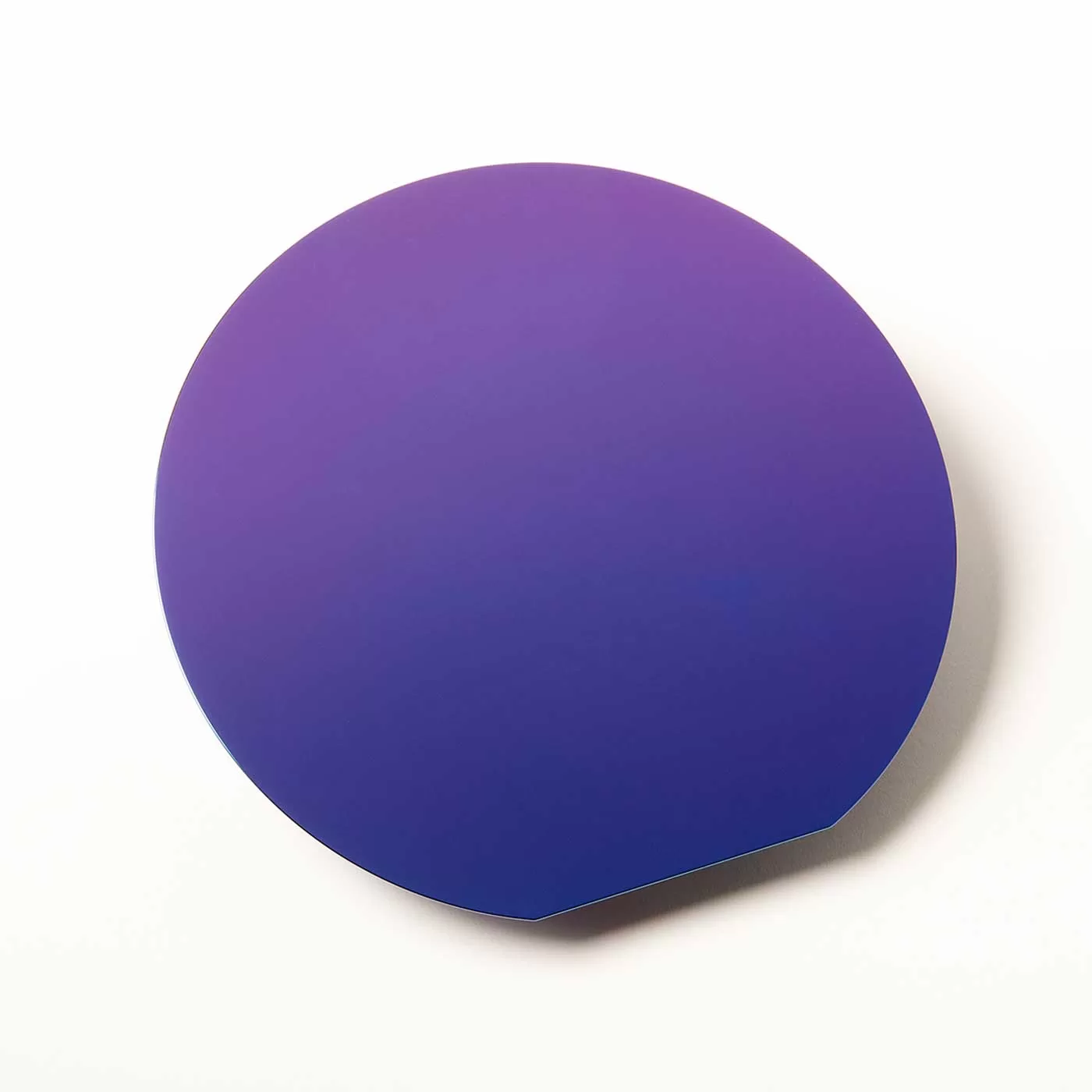
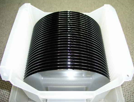
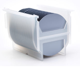
CZ-Si Wafers’ showcase
CZ-Si Wafers’ properties
CZ-Si (Czochralski Silicon) wafers are integral to the modern semiconductor industry, renowned for their exceptional properties that enable a wide array of applications across various technological sectors. These wafers are manufactured using the Czochralski process, a method that yields high-purity silicon crystals with excellent crystal quality and uniform electrical characteristics. Here, we delve into the properties and significance of CZ-Si wafers in detail.
- High Purity: CZ-Si wafers boast an extremely high level of purity, with impurity concentrations typically measured in parts per billion (ppb). This purity is crucial for ensuring the reliability and performance of semiconductor devices, as even minute impurities can adversely affect their functionality.
- Excellent Crystal Quality: The Czochralski process allows for the growth of silicon crystals with superior crystal quality. This results in wafers characterized by uniform crystal structures and minimal crystal defects, such as dislocations and stacking faults. The absence of such defects is essential for achieving high device yields and operational reliability in semiconductor manufacturing.
- Uniform Electrical Properties: CZ-Si wafers exhibit uniform electrical properties across their entire surface, ensuring consistent device performance. This uniformity is vital for the fabrication of integrated circuits (ICs) and other semiconductor devices, where precise control over electrical characteristics is paramount.
- Large Wafer Diameters: CZ-Si wafers are available in a range of diameters, with larger diameters becoming increasingly prevalent in semiconductor fabrication facilities. Larger wafers enable higher device throughput per batch and reduce manufacturing costs per unit, contributing to enhanced efficiency and cost-effectiveness in semiconductor production.
- Tailored Doping Profiles: Doping, the process of intentionally introducing impurities into the silicon crystal lattice, is utilized to modify the electrical properties of CZ-Si wafers. Through precise doping control, semiconductor manufacturers can tailor the electrical conductivity and characteristics of the wafers to suit specific device requirements.
- Optical Transparency: In addition to their electrical properties, CZ-Si wafers also exhibit excellent optical transparency in the infrared spectrum. This transparency is advantageous for applications such as infrared imaging devices and optoelectronic sensors, where silicon substrates must allow the passage of infrared light.
- Thermal Stability: CZ-Si wafers possess excellent thermal stability, with minimal changes in electrical properties over a wide temperature range. This thermal stability is crucial for maintaining device performance under varying operating conditions and thermal environments.
- Chemical Inertness: Silicon, the primary constituent of CZ-Si wafers, is inherently chemically inert, making the wafers resistant to corrosion and degradation when exposed to most chemicals. This chemical inertness enhances the reliability and longevity of semiconductor devices fabricated on CZ-Si substrates.
- Compatibility with Semiconductor Processes: CZ-Si wafers are compatible with a wide range of semiconductor manufacturing processes, including photolithography, etching, deposition, and doping. This compatibility facilitates the integration of CZ-Si wafers into existing semiconductor fabrication workflows, enabling seamless production of advanced semiconductor devices.
- Versatility in Applications: Owing to their exceptional properties, CZ-Si wafers find widespread applications across various industries. They are indispensable in the production of integrated circuits (ICs), optoelectronic devices (such as light-emitting diodes and photodetectors), photovoltaic cells (solar panels), and microelectromechanical systems (MEMS) devices. As electronic technology continues to advance, the demand for CZ-Si wafers is expected to grow, driving innovation and progress in semiconductor technology and contributing to the development of new and emerging applications.
In summary,
Physical property
- State of matter: solid
- Melting point: 1687K (1414 ℃)
- Boiling point: 3173K (2900 ° C)
- Molar volume: 12.06 × 10⁻⁶m3 / mol
- vaporization heat: 384.22kJ / mol
- Melting heat: 50.55kJ / mol
- Vapor pressure: 4.77Pa (1683K)
CZ-Si wafers represent a cornerstone of modern semiconductor manufacturing, offering unparalleled purity, crystal quality, and electrical uniformity. Their diverse properties and compatibility with semiconductor processes make them indispensable components in a wide range of electronic and optoelectronic devices, driving innovation and advancement in technology across various industries.