
描述
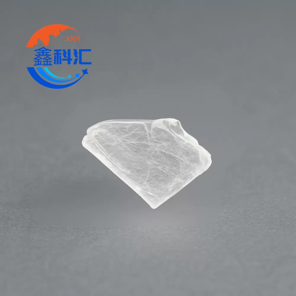
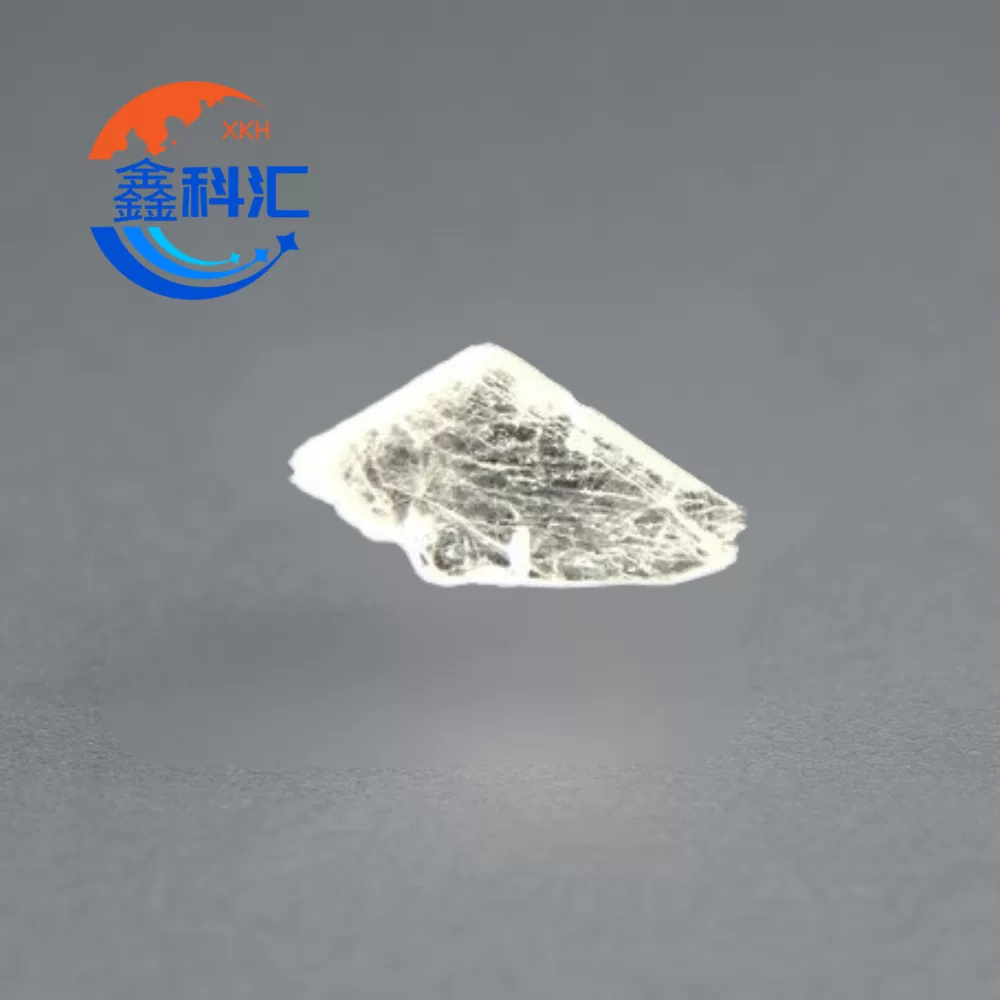
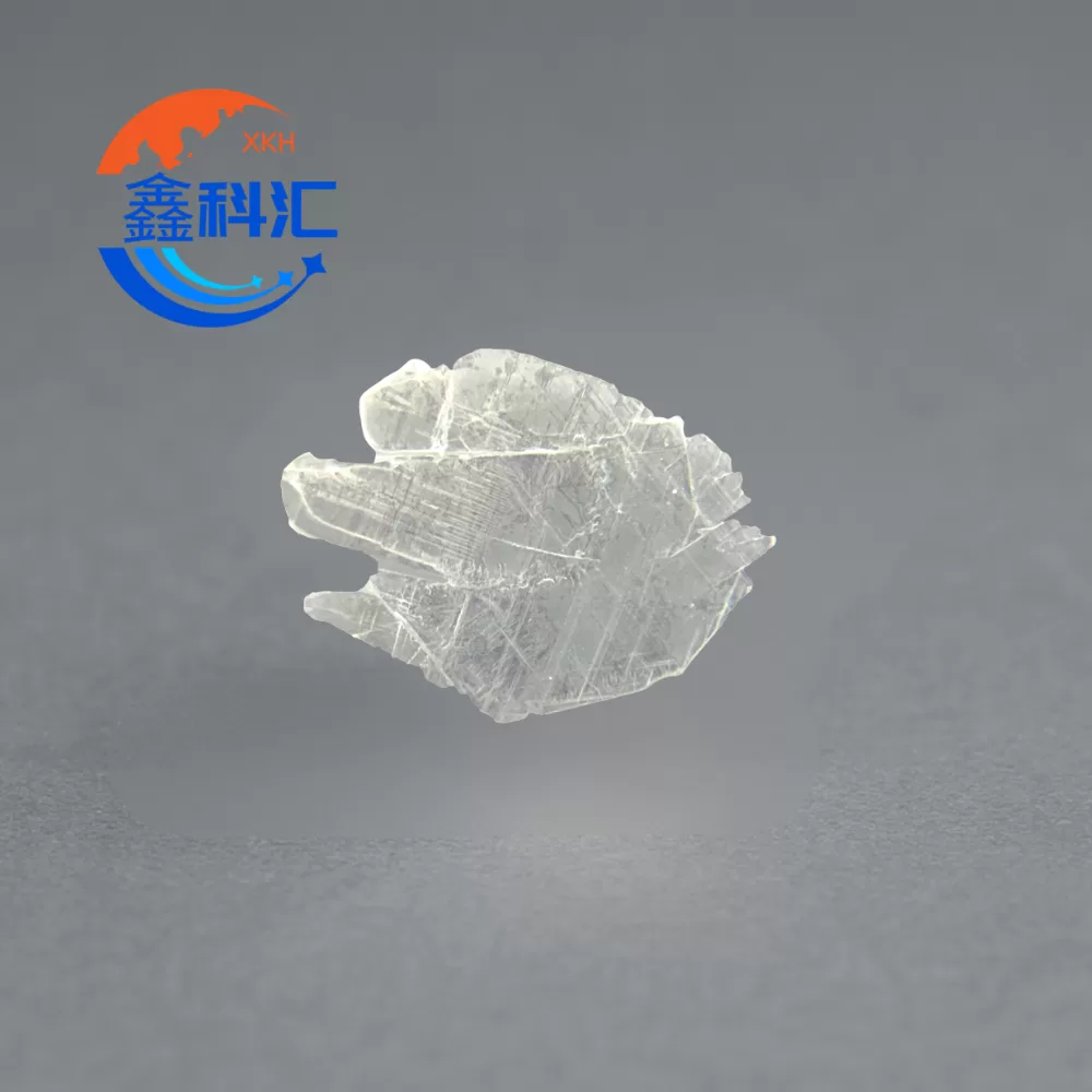
Device-Grade hBN Single Crystal is a premium hexagonal boron nitride material developed for advanced semiconductor research, two-dimensional materials, graphene electronics, and next-generation photonic devices. Produced through a proprietary crystal growth process under atmospheric pressure, these high-quality hBN crystals exhibit excellent crystallinity, low defect density, outstanding dielectric properties, and exceptional optical performance.
As a wide-bandgap layered material, hBN has become one of the most important building blocks in the rapidly growing field of two-dimensional materials. Its atomically smooth surface, chemical stability, and superior electrical insulation make it an ideal substrate and encapsulation layer for graphene and other van der Waals materials.
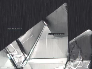
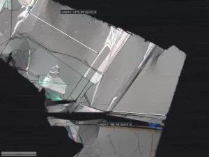
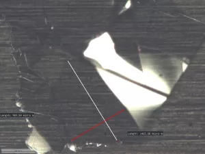
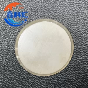
Our device-grade hBN crystals are supplied as millimeter-scale bulk single crystals with natural growth facets, providing researchers and technology developers with a reliable platform for high-performance device fabrication.
Key Benefits
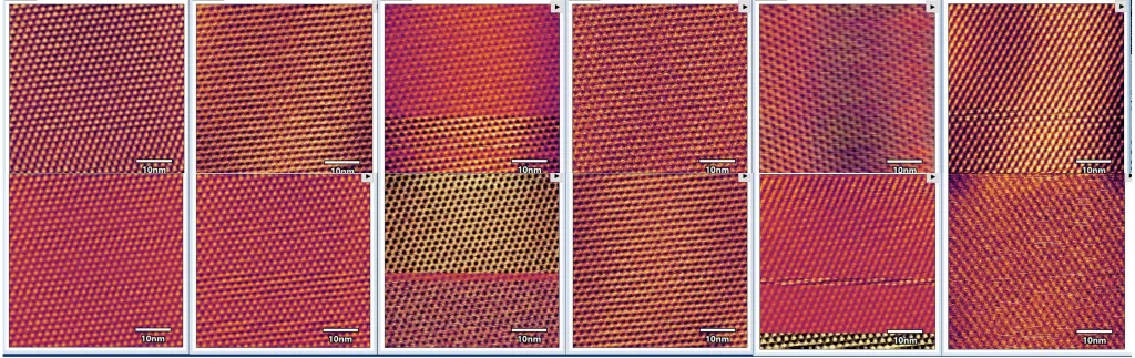
Exceptional Crystal Quality
Carefully controlled crystal growth results in large single-crystal domains with excellent structural integrity and low impurity levels.
Ideal for Graphene Devices
The atomically flat surface minimizes carrier scattering and supports ultra-high mobility graphene electronic devices.
Excellent Electrical Insulation
High dielectric breakdown strength enables reliable operation in advanced nanoelectronic and quantum devices.
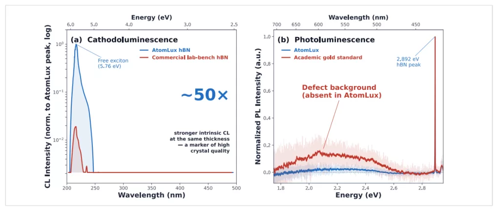
Superior Optical Properties
The material demonstrates strong ultraviolet band-edge emission and excellent optical characteristics suitable for photonic applications.
Easy Exfoliation
The layered crystal structure allows the preparation of thin hBN flakes for research and device fabrication.
Technische Daten
| Eigentum | Wert |
|---|---|
| Material | Hexagonal Boron Nitride (hBN) |
| Crystal Type | Single Crystal |
| Klasse | Device Grade |
| Wachstum Methode | Proprietary Atmospheric-Pressure Growth |
| Crystal Form | Bulk Crystal |
| Typical Lateral Size | ≥ 1 mm |
| Surface Condition | Natural Growth Surface |
| Package Type | Chip Carrier |
| Quantity per Package | 5–10 Crystals |
Electrical Characteristics
| Parameter | Typischer Wert |
| Dielectric Breakdown Field | 1.64 ± 0.06 V/nm |
Optical Characteristics
| Parameter | Typischer Wert |
| UV Band-Edge Emission | Approximately 215 nm |
| Optical Transparency | Hoch |
| Luminescence Quality | Advanced Research Grade |
Raman Properties
| Parameter | Typischer Wert |
| E₂g Raman Peak Linewidth | 7.88 cm⁻¹ |
Graphene Device Reference Performance
| Parameter | Typischer Wert |
| Graphene Mobility at Room Temperature | Approximately 80,000 cm²/V·s |
| Carrier Density | 1 × 10¹² cm⁻² |
Anwendungen
Graphene Electronics
Widely used as an ultra-flat substrate and encapsulation layer for graphene transistors, sensors, and high-speed electronic devices.
Two-Dimensional Material Research
Suitable for constructing van der Waals heterostructures involving graphene, MoS₂, WS₂, WSe₂, and other layered materials.
Quantum Devices
Provides an ideal platform for quantum transport studies, correlated electronic systems, and advanced quantum technologies.
Nanophotonics
Supports phonon-polariton phenomena and nanoscale light manipulation for next-generation photonic devices.
Deep Ultraviolet Technologies
The intrinsic UV emission properties of hBN make it attractive for deep-UV detectors, emitters, and optical research.
Advanced Semiconductor Research
Used in universities, national laboratories, and industrial R&D centers working on future semiconductor technologies.
Why Choose Device-Grade hBN Single Crystal?
- High-purity single-crystal material
- Large usable crystal domains
- Excellent electrical insulation
- Outstanding optical properties
- Proven performance in graphene devices
- Suitable for advanced research and prototype development
- Reliable packaging and handling
- Available for customized selection
Packaging Information
Device-Grade hBN Single Crystals are carefully packaged in protective chip carriers to prevent contamination and mechanical damage during transportation and storage.
Customized packaging and crystal selection services are available according to customer requirements.
FAQ
What is Device-Grade hBN?
Device-grade hBN is a high-quality single-crystal form of hexagonal boron nitride specifically developed for advanced electronic, photonic, and quantum device applications.
Why is hBN important for graphene research?
Its atomically smooth and electrically insulating surface enables graphene devices to achieve significantly improved carrier mobility and overall performance.
Can hBN be used as a substrate material?
Yes. hBN is one of the most widely used substrate materials for graphene, two-dimensional materials, and van der Waals heterostructures.
What crystal size is available?
Standard crystals typically provide lateral dimensions greater than 1 mm. Custom crystal selection may be available upon request.
Is this material suitable for academic and industrial research?
Yes. Device-grade hBN single crystals are widely used in universities, research institutes, semiconductor laboratories, and advanced technology development programs worldwide.

Rezensionen
Es gibt noch keine Rezensionen.