
This document presents an overview of our 4-inch silicon carbide (SiC) wafers, specifically designed for high-performance applications in power electronics and optoelectronics. Available in both N-Type and semi-insulating variants, these 4H-SiC substrates exhibit superior electrical properties, thermal conductivity, and chemical stability, making them ideal for demanding environments.
Silicon carbide is recognized for its ability to operate at high voltages, temperatures, and frequencies, positioning it as a critical material for next-generation devices such as power transistors, diodes, and high-frequency RF devices. Our Silicon Carbide wafers feature excellent surface quality, low defect density, and uniform thickness, ensuring optimal performance in semiconductor fabrication processes.
With their robust characteristics, our Silicon Carbide wafers are poised to meet the increasing demands of various industries, including automotive, telecommunications, and renewable energy. This paper will delve into the specifications, benefits, and applications of these silicon carbide substrates, highlighting their role in advancing technological innovation and efficiency in modern electronic systems.
4 inch Silicon Carbide wafer (SiC) Crystal Substrate, SiC Wafers Specifications
| Parametri | Nolla MPD-luokka | Tuotantoluokka | Tutkimusaste | Dummy-luokka |
|---|---|---|---|---|
| Halkaisija | 100.0 mm +/- 0.5 mm | 100.0 mm +/- 0.5 mm | 100.0 mm +/- 0.5 mm | 100.0 mm +/- 0.5 mm |
| Paksuus | 500 um +/- 25 um (semi-insulating) | 350 um +/- 25 um (N type) | 500 um +/- 25 um (semi-insulating) | 350 um +/- 25 um (N type) |
| Kiekon suuntaus | On axis: <0001> +/- 0.5 deg for 4H-SI | On axis: <0001> +/- 0.5 deg for 4H-SI | On axis: <0001> +/- 0.5 deg for 4H-SI | On axis: <0001> +/- 0.5 deg for 4H-SI |
| Off axis: 4.0 deg toward <11-20> +/-0.5 deg for 4H-N | Off axis: 4.0 deg toward <11-20> +/-0.5 deg for 4H-N | Off axis: 4.0 deg toward <11-20> +/-0.5 deg for 4H-N | Off axis: 4.0 deg toward <11-20> +/-0.5 deg for 4H-N | |
| Micropipe Density (MPD) | 1 cm⁻² | 5 cm⁻² | 15 cm⁻² | 30 cm⁻² |
| Electrical Resistivity (Ohm-cm) | 4H-N: 0.015~0.028 | 4H-N: 0.015~0.028 | 4H-N: 0.015~0.028 | 4H-N: 0.015~0.028 |
| 4H-SI: >1E5 | 4H-SI: >1E5 | 4H-SI: >1E5 | 4H-SI: >1E5 | |
| Doping Concentration | N-type: ~ 1E18/cm³ | N-type: ~ 1E18/cm³ | N-type: ~ 1E18/cm³ | N-type: ~ 1E18/cm³ |
| SI-type (V-doped): ~ 5E18/cm³ | SI-type (V-doped): ~ 5E18/cm³ | SI-type (V-doped): ~ 5E18/cm³ | SI-type (V-doped): ~ 5E18/cm³ | |
| Ensisijainen asunto | {10-10} +/- 5.0 deg | {10-10} +/- 5.0 deg | {10-10} +/- 5.0 deg | {10-10} +/- 5.0 deg |
| Ensisijainen litteä pituus | 32.5 mm +/- 2.0 mm | 32.5 mm +/- 2.0 mm | 32.5 mm +/- 2.0 mm | 32.5 mm +/- 2.0 mm |
| Toissijainen tasainen pituus | 18.0 mm +/- 2.0 mm | 18.0 mm +/- 2.0 mm | 18.0 mm +/- 2.0 mm | 18.0 mm +/- 2.0 mm |
| Toissijainen tasainen suuntaus | Silicon face up: 90 deg CW from Primary flat +/- 5.0 deg | Silicon face up: 90 deg CW from Primary flat +/- 5.0 deg | Silicon face up: 90 deg CW from Primary flat +/- 5.0 deg | Silicon face up: 90 deg CW from Primary flat +/- 5.0 deg |
| Edge Exclusion | 3 mm | 3 mm | 3 mm | 3 mm |
| LTV/TTV /Bow /Warp | 10 um / 15 um / 25 um / 40 um | 10 um / 15 um / 25 um / 40 um | 10 um / 15 um / 25 um / 40 um | 10 um / 15 um / 25 um / 40 um |
| Pinnan karheus | Optical Polish Ra < 1 nm on the C face | Optical Polish Ra < 1 nm on the C face | Optical Polish Ra < 1 nm on the C face | Optical Polish Ra < 1 nm on the C face |
| CMP Ra < 0.5 nm on the Si face | CMP Ra < 0.5 nm on the Si face | CMP Ra < 0.5 nm on the Si face | CMP Ra < 0.5 nm on the Si face | |
| Cracks Inspected by High Intensity Light | Ei ole | Ei ole | 1 allowed, 1 mm | 1 allowed, 2 mm |
| Hex Plates Inspected by High Intensity Light | Cumulative area 1% | Cumulative area 1% | Cumulative area 1% | Cumulative area 3% |
| Polytype Areas Inspected by High Intensity Light | Ei ole | Ei ole | Cumulative area 2% | Cumulative area 5% |
| Scratches Inspected by High Intensity Light | 3 scratches to 1 x wafer diameter cumulative length | 3 scratches to 1 x wafer diameter cumulative length | 5 scratches to 1 x wafer diameter cumulative length | 5 scratches to 1 x wafer diameter cumulative length |
| Edge Chipping | Ei ole | Ei ole | 3 allowed, 0.5 mm each | 5 allowed, 1 mm each |
| Surface Contamination as Inspected by High Intensity Light | Ei ole | Ei ole | Ei ole | Ei ole |
4 inch Silicon Carbide wafer (SiC) Crystal Substrate PROPERTIES OF SILICON CARBIDE CRYSTAL MATERIALS
| Kiinteistö | 4H-SiC Single Crystal | 6H-SiC Single Crystal |
|---|---|---|
| Lattice Parameters (Å) | a = 3.076, c = 10.053 | a = 3.073, c = 15.117 |
| Stacking Sequence | ABCB | ABCACB |
| Tiheys | 3.21 | 3.21 |
| Mohs Hardness | ~9.2 | ~9.2 |
| Thermal Expansion Coefficient (CTE) (/K) | 4-5 x 10⁻⁶ | 4-5 x 10⁻⁶ |
| Refraction Index @ 750nm | no = 2.61, ne = 2.66 | no = 2.60, ne = 2.65 |
| Dielektrinen vakio | c ~ 9.66 | c ~ 9.66 |
| Doping Type | N-type or Semi-insulating | N-type or Semi-insulating |
| Thermal Conductivity (W/cm-K @ 298K) | (N-type, 0.02 ohm-cm) a ~ 4.2, c ~ 3.7 | a ~ 4.6, c ~ 3.2 |
| Thermal Conductivity (W/cm-K @ 298K) | (Semi-insulating type) a ~ 4.9, c ~ 3.9 | – |
| Band-gap (eV) | 3.23 | 3.02 |
| Break-Down Electrical Field (V/cm) | 3-5 x 10⁶ | 3-5 x 10⁶ |
| Saturation Drift Velocity (m/s) | 2.0 x 10⁵ | 2.0 x 10⁵ |
| Wafer and Substrate Sizes | Wafers: 2, 4, 6, 8 inch; smaller substrates: 10×10, 20×20 mm, other sizes available upon request | – |
| Product Grades | A Grade: Zero micropipe density (MPD 1 cm⁻²) B Grade: Production grade (MPD 5 cm⁻²) C Grade: Research grade (MPD 15 cm⁻²) D Grade: Dummy grade (MPD 30 cm⁻²) | – |
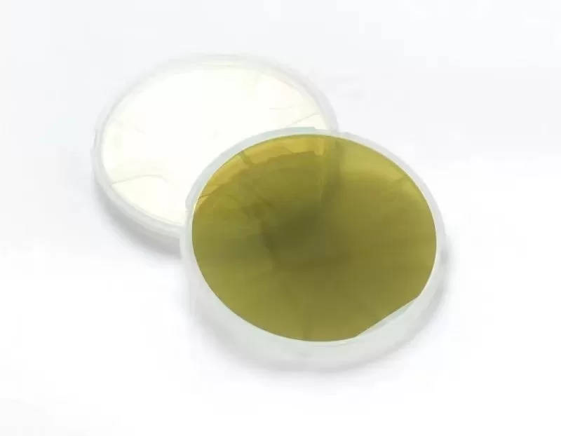
4 inch Silicon Carbide wafer’s photo
4 inch Silicon Carbide wafer’s application
Here’s a more extensive overview of applications for 4-inch Silicon Carbide (SiC) wafers, along with additional details for each category:
1. Tehoelektroniikka
- MOSFETs and Diodes: Silicon Carbide wafers is favored for high-voltage MOSFETs and Schottky diodes due to its wide bandgap and high breakdown voltage, which allow devices to operate at higher temperatures and frequencies. Applications include:
- Inverters: Used in renewable energy systems and electric vehicles (EVs) to convert DC to AC power efficiently.
- Converters: Silicon Carbide wafers Essential in power management systems, including battery chargers and power supplies.
2. High-Temperature Applications
- Aerospace and Defense: Silicon Carbide wafers can withstand extreme temperatures and radiation, making them suitable for applications in satellites, avionics, and military electronics.
- Oil and Gas Exploration: High-performance sensors made from SiC can function in the harsh environments found in drilling operations.
3. RF and Microwave Devices
- High-Frequency Amplifiers: Silicon Carbide wafers ability to operate at microwave frequencies makes it ideal for RF amplifiers used in communication systems, satellite communications, and radar technology.
- Gallium Nitride (GaN) Integration: SiC can be integrated with GaN devices to enhance performance in high-power RF applications.
4. LEDs and Photovoltaics
- High-Power LEDs: Silicon Carbide wafers can improve the performance and efficiency of blue and UV LEDs, used in lighting and displays.
- Solar Cells: SiC can enhance the efficiency and thermal stability of solar cells, particularly in concentrated solar power systems.
5. Electric Vehicles (EVs)
- Onboard Chargers: SiC devices enable smaller, lighter, and more efficient onboard chargers, reducing the weight and volume of EVs.
- Traction Inverters:Silicon Carbide wafers improve the efficiency and performance of electric motors in EVs, enhancing acceleration and range.
- Battery Management Systems: SiC enhances the reliability and efficiency of systems managing battery health and performance.
6. Industrial Automation
- Servo Drives: Silicon Carbide waferstechnology is used in high-performance servo drives for robotics and automation, providing better torque and speed control.
- Variable Frequency Drives (VFDs): Used in electric motors across various industries to improve energy efficiency.
7. Renewable Energy Systems
- Wind Turbines: SiC devices enhance the efficiency of power conversion systems in wind turbines, allowing for higher energy capture and better grid integration.
- Smart Grid Applications: Silicon Carbide wafers technology supports advanced energy management systems, improving the efficiency of energy distribution.
8. Medical Devices
- Sensors: SiC-based sensors can operate in harsh environments and provide reliable measurements in medical equipment.
- Implantable Devices: Biocompatibility and durability make SiC suitable for applications in pacemakers and other implantable electronics.
9. Telecommunications
- Base Stations: SiC technology is used in amplifiers for cellular base stations, enhancing signal strength and coverage.
- Tietokeskukset: Silicon Carbide wafers devices can improve the efficiency of power supplies in data centers, reducing energy consumption and heat generation.
10. Consumer Electronics
- Smart Chargers: SiC technology can enhance the performance of fast chargers for smartphones and laptops, providing quicker charging times with lower heat output.
- Home Appliances: SiC devices are increasingly used in energy-efficient appliances, reducing overall energy consumption.
11. Automotive Applications
- Battery Electric and Hybrid Vehicles: SiC is used in electric powertrains, allowing for improved efficiency and thermal management.
- Advanced Driver-Assistance Systems (ADAS): SiC technology enhances the reliability and performance of sensors and control systems.
12. Electric Grid Management
- Grid Stabilization: SiC-based devices contribute to improved grid stability and management by enabling faster response times and better power quality.
13. Smart Manufacturing
- Industry 4.0: SiC technology supports the development of smart manufacturing solutions, allowing for better energy efficiency and process optimization.
14. Testing and Measurement
- High-Precision Instruments: Silicon Carbide wafers are used in precision instruments for testing and measurement applications in various scientific and industrial contexts.
These applications demonstrate the versatility and wide-ranging impact of 4-inch SiC wafers across multiple industries, driving advancements in efficiency, performance, and sustainability. If you need further details on any specific application or technology, feel free to ask!
4 inch Silicon Carbide wafer’s properties
Silicon Carbide (SiC) wafers possess a range of unique properties that make them highly suitable for various advanced applications, particularly in power electronics and high-temperature environments. Here are some key properties of SiC wafers:
1. Wide Bandgap
- Silicon Carbide wafers a wide bandgap of about 3.0 to 3.3 eV, allowing it to operate at higher voltages and temperatures compared to silicon. This characteristic enables devices to switch faster and handle more power, reducing energy losses.
2. Korkea lämmönjohtavuus
- Silicon Carbide wafers exhibits excellent thermal conductivity (around 3.5 W/cm·K), which helps in effective heat dissipation. This property is crucial for power devices that generate significant heat during operation, improving reliability and efficiency.
3. Korkea hajoamissähkökenttä
- Silicon Carbide wafers can withstand high electric fields, with a breakdown field strength of around 3-5 MV/cm. This allows for the design of devices that can operate at higher voltages, making SiC ideal for high-power applications.
4. Korkea mekaaninen lujuus
- SiC has a high Young’s modulus and is mechanically strong, making it resistant to deformation and wear. This durability is beneficial in harsh environments and for demanding applications.
5. Excellent Chemical Stability
- Silicon Carbide wafers chemically inert and resistant to corrosion, which enhances its performance in hostile environments, including high-temperature and high-humidity conditions.
6. Low Thermal Expansion Coefficient
- The coefficient of thermal expansion for SiC is lower than that of silicon, reducing the risk of thermal stress and enhancing the reliability of devices during thermal cycling.
7. High Saturation Drift Velocity
- Silicon Carbide wafers have a high saturation drift velocity (about 2 x 10^5 m/s), allowing for faster switching speeds in power devices, which is essential for efficient power conversion.
8. Doping Capability
- SiC can be doped with various impurities to create n-type or p-type semiconductors, enabling a wide range of electronic device applications. Common dopants include nitrogen (for n-type) and aluminum (for p-type).
9. Pinnan karheus
- Silicon Carbide wafers can be produced with low surface roughness, which is critical for high-performance electronic and optoelectronic devices. Surface roughness can vary based on the manufacturing process (e.g., optical polish or chemical mechanical planarization).
10. Resistiivisyys
- The electrical resistivity of Silicon Carbide wafers can vary significantly depending on the doping concentration, making it versatile for different applications. N-type SiC can have resistivities as low as 0.015-0.028 ohm-cm, while semi-insulating types can exceed 1 x 10^5 ohm-cm.
11. Lattice Structure
- SiC can exist in multiple polytypes, such as 4H-SiC and 6H-SiC, each with distinct properties. The 4H-SiC structure is commonly used for power devices due to its favorable electronic properties.
12. Dielektrinen vakio
- The dielectric constant of SiC is around 9.66, which is beneficial for high-frequency applications and for minimizing capacitance in electronic circuits.
13. Optiset ominaisuudet
- SiC exhibits good optical properties, including a high refractive index, which is advantageous for optoelectronic devices, including LEDs and photodetectors.
14. Mikroputken tiheys
- The density of micropipes (defects in the crystal structure) can affect the performance of SiC wafers. High-quality SiC wafers have low micropipe density, contributing to better device performance.
These properties make Silicon Carbide wafers highly desirable for advanced electronics, particularly in high-power, high-temperature, and high-frequency applications. If you need specific information or further details on any property, feel free to ask!
4 inch Silicon Carbide wafer’s Q&A
What is a silicon carbide wafer used for?
Silicon carbide (SiC) wafers are increasingly used in various high-performance applications due to their unique properties, such as a wide bandgap, high thermal conductivity, and excellent mechanical strength. Here are some of the primary applications of silicon carbide wafers:
1. Tehoelektroniikka
- SiC wafers are widely used in power devices such as MOSFETs, diodes, and IGBTs. These devices are critical for efficient power conversion in applications like power supplies, electric vehicles, and renewable energy systems.
2. High-Temperature Applications
- Due to their high thermal stability,Silicon Carbide wafers are suitable for high-temperature environments, making them ideal for aerospace, automotive, and industrial applications where devices must operate reliably at elevated temperatures.
3. RF and Microwave Devices
- Silicon carbide is used in RF (radio frequency) and microwave applications, including amplifiers and transistors, which benefit from Silicon Carbide wafers’s ability to operate at high frequencies and voltages.
4. LEDs and Optoelectronics
- While traditional LEDs are often made from gallium nitride (GaN), SiC is sometimes used in the production of high-power LED applications, especially in lighting and display technologies.
5. Electric Vehicles (EVs)
- Silicon Carbide wafers are crucial for the development of EV powertrains, enabling more efficient charging systems, inverters, and battery management systems that enhance the performance and range of electric vehicles.
6. Telecommunications
- In telecommunications infrastructure, SiC is used in power amplifiers and other components that require high efficiency and reliability, supporting high-frequency signals.
7. Industrial Equipment
- SiC wafers are utilized in industrial power control systems, such as motor drives and robotics, where efficiency and thermal management are critical.
8. High-Power Lasers
- SiC is used in certain high-power laser systems, benefiting from its ability to handle high heat loads and provide stability in challenging environments.
9. Sensor Applications
- Silicon carbide is used in high-temperature sensors and devices that require reliability and performance in extreme conditions, including automotive and aerospace sensors.
10. Durable Substrates
- SiC wafers can serve as substrates for other materials, providing a robust platform for the growth of various semiconductor layers, particularly in compound semiconductors.
11. Photovoltaics
- Although not as common as silicon for solar cells, SiC wafers can be used in specialized photovoltaic applications, particularly in environments where high efficiency and thermal management are crucial.
12. Research and Development
- SiC wafers are used in research settings to develop and test new semiconductor devices and materials, contributing to advancements in electronics and materials science.
13. Silicon Carbide Fiber Reinforcement
- In composite materials, SiC wafers can be used to create SiC fibers that reinforce other materials, improving their mechanical properties and thermal stability.
Silicon carbide wafers are a key enabler in the transition toward more efficient, high-performance electronic systems, particularly in the context of emerging technologies like electric vehicles and renewable energy. If you need more information about any specific application, let me know!
What is the difference between silicon and SiC?
Silicon (Si) and silicon carbide (SiC) are both important materials in the semiconductor industry, but they have distinct properties and applications. Here are the key differences between the two:
1. Kiderakenne
- Silicon: Has a diamond cubic crystal structure, which is a single-element semiconductor.
- Piikarbidi: Exists in several polytypes (e.g., 4H-SiC, 6H-SiC) with different arrangements of silicon and carbon atoms, giving it unique properties.
2. Bandgap
- Silicon: Has a bandgap of about 1.12 eV, which limits its performance at high temperatures and voltages.
- Piikarbidi: Has a wider bandgap (about 3.0 to 3.3 eV), allowing it to operate at higher temperatures and voltages with reduced energy losses.
3. Lämmönjohtavuus
- Silicon: Has moderate thermal conductivity (~150 W/m·K), which can limit its performance in high-power applications.
- Piikarbidi: Exhibits high thermal conductivity (~3.5 W/cm·K), enabling efficient heat dissipation in high-power devices.
4. Sähköiset ominaisuudet
- Silicon: More susceptible to thermal runaway and has lower breakdown voltage (typically around 0.3 MV/cm).
- Piikarbidi: Has a much higher breakdown electric field (3-5 MV/cm), making it suitable for high-voltage applications.
5. Doping Characteristics
- Silicon: Can be easily doped with elements like phosphorus (n-type) or boron (p-type) to create semiconductors.
- Piikarbidi: Can also be doped, but the process is more complex due to its wider bandgap and different crystallographic structures.
6. Sovellukset
- Silicon: Dominates in traditional electronics, microprocessors, and standard semiconductor devices due to its established manufacturing processes and cost-effectiveness.
- Piikarbidi: Gaining prominence in high-power, high-temperature, and high-frequency applications, such as power electronics, electric vehicles, and RF devices, where silicon’s limitations become significant.
7. Kustannukset
- Silicon: Generally less expensive and more widely available due to mature manufacturing processes and infrastructure.
- Piikarbidi: More expensive to produce, partly due to the complexities of growing high-quality SiC crystals and the relative newness of the technology.
8. Mekaaniset ominaisuudet
- Silicon: Has lower mechanical strength and is more brittle compared to SiC.
- Piikarbidi: Offers higher mechanical strength and hardness, making it suitable for applications requiring durability.
9. Lämpölaajenemiskerroin
- Silicon: Has a higher thermal expansion coefficient compared to SiC, which can lead to challenges in thermal management in high-temperature applications.
- Piikarbidi: Has a lower thermal expansion coefficient, reducing thermal stress and enhancing reliability in high-temperature environments.
Yhteenveto
In summary, while silicon is the traditional material for semiconductor devices, silicon carbide offers significant advantages for high-performance applications, particularly in power electronics and environments where higher temperatures and voltages are required. The choice between the two materials depends on the specific requirements of the application. If you have any more questions or need further details, feel free to ask!