
In advanced semiconductor packaging, MEMS devices, optical sensors, and high-frequency electronic systems, device structures are gradually moving from traditional two-dimensional layouts toward three-dimensional integration. To achieve shorter signal paths, higher integration density, and more compact device architectures, vertical interconnection technologies have become increasingly important.
One important concept in this field is TGV, which stands for Through Glass Via. In its strict definition, TGV refers to vertical through-holes formed in glass substrates, often used for electrical interconnection, packaging, or structural integration.
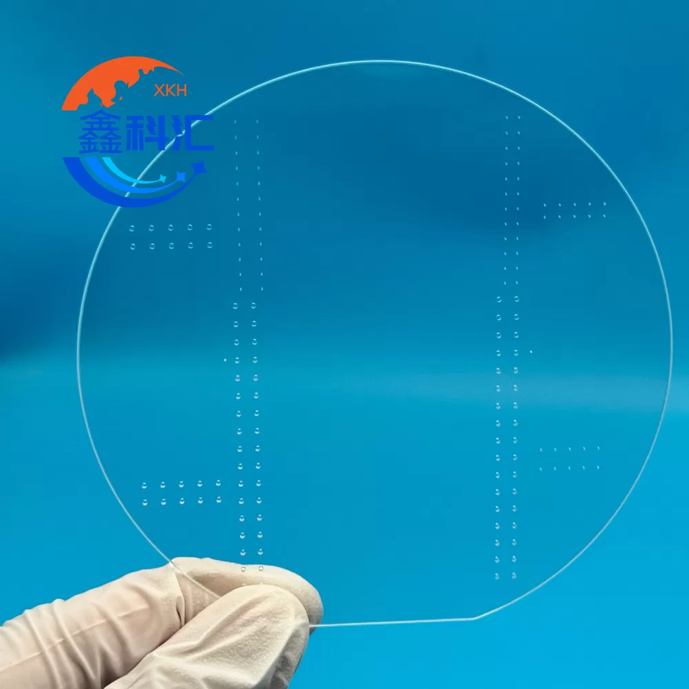
However, when we discuss a TGV Sapphire Substrate, the meaning is slightly different. Sapphire is not ordinary glass. It is a single-crystal aluminum oxide material with the chemical formula Al₂O₃. Therefore, the term TGV Sapphire Substrate usually refers to a sapphire wafer or sapphire plate processed with TGV-like through-via structures, such as micro holes, through-hole arrays, square openings, alignment holes, and patterned cavities.
In other words, it is a precision-machined sapphire substrate with vertical through structures, designed for advanced packaging, MEMS, optical, sensor, and high-reliability electronic applications.
1. What Is a TGV Sapphire Substrate?
A TGV Sapphire Substrate is a sapphire wafer or sapphire plate processed with micro-scale through structures. These structures may include:
| Structure Type | Function |
|---|---|
| Through Via Holes | Vertical connection, alignment, or structural integration |
| Micro Hole Arrays | Sensor structures, microfluidic channels, packaging design, or positioning |
| Square Windows | Optical transmission, chip exposure, or device packaging |
| Alignment Holes | Assembly, bonding, testing, or precision positioning |
| Patterned Cavities | MEMS, microfluidic, optical, or sensor applications |
If the through holes are later metallized, coated, or filled with conductive material, the substrate may also be used as part of a vertical electrical interconnection structure. Without metallization, the sapphire substrate can still function as a high-strength optical, mechanical, insulating, or microstructured carrier.
2. Why Use Sapphire Instead of Ordinary Glass?
Traditional TGV substrates are often made from borosilicate glass, quartz glass, or other glass materials. These materials are widely used because they are insulating, transparent, and compatible with certain microfabrication processes.
Sapphire, however, offers a much higher level of mechanical and environmental performance. It is especially useful when the application requires high strength, excellent scratch resistance, chemical durability, and thermal stability.
| Sapphire Property | Importance for TGV-Like Structures |
|---|---|
| Dureté élevée | Improves scratch resistance and wear resistance |
| Haute résistance mécanique | Helps maintain structural stability in thin substrates |
| Transparence optique | Suitable for optical sensors, windows, and inspection systems |
| Isolation électrique | Useful for electronic, RF, and packaging substrates |
| Stabilité thermique | Suitable for high-temperature processing or operation |
| Résistance chimique | Performs well in harsh or corrosive environments |
| Single-Crystal Structure | Provides stable and consistent material behavior |
For applications where ordinary glass may be too fragile or insufficiently durable, sapphire can provide a more robust substrate platform.
3. Key Manufacturing Challenges
Although sapphire has excellent material properties, it is also difficult to process. Its high hardness and chemical stability make micro-hole drilling, cutting, polishing, and patterning more challenging than with ordinary glass.
3.1 Micro Hole Processing
Micro holes in sapphire are commonly produced by laser drilling, ultrafast laser processing, precision grinding, or combined machining methods. Important quality factors include:
- Hole diameter
- Hole pitch
- Hole taper
- Ébarbage des bords
- Microcracks
- Heat-affected zone
- Hole wall roughness
- Positional accuracy
For TGV-style substrates, hole quality is critical. Poor hole wall quality or edge damage may affect later metallization, bonding, optical performance, or mechanical reliability.
3.2 Surface Polishing
Sapphire substrates often require precise surface polishing. Surface quality is especially important for optical devices, MEMS components, wafer bonding, and packaging applications.
Common surface options include:
- Single-side polished surface
- Double-side polished surface
- Customized roughness
- Optical-grade polishing
- Local window polishing
- Edge grinding and chamfering
Flatness, roughness, and surface defects must be carefully controlled according to the final application.
3.3 Via Metallization
If the TGV sapphire substrate is used for electrical interconnection, the through holes must be metallized or filled with conductive material. Since sapphire itself is an insulating material, the via structure only becomes electrically functional after additional processing.
A typical metallization process may involve:
- Cleaning and activation of the hole wall
- Deposition of an adhesion layer
- Seed layer deposition
- Metal coating or electroplating
- Via filling or conformal coating
- Annealing and reliability testing
This process is more complex than simple hole drilling. Adhesion, thermal expansion mismatch, metal continuity, and long-term reliability must all be considered.
4. Important Design Parameters
When designing or purchasing a TGV sapphire substrate, it is not enough to specify only the hole diameter. The entire substrate structure should be evaluated as a system.
| Paramètres | Description |
|---|---|
| Substrate Size | Round wafer, square plate, rectangular plate, or custom shape |
| Épaisseur | Affects strength, transparency, and via processing difficulty |
| Hole Diameter | Determines function, processing complexity, and metallization feasibility |
| Hole Pitch | Influences array density and mechanical strength |
| Hole Quantity | Affects cost, processing time, and yield |
| Hole Taper | Important for assembly, coating, and via uniformity |
| Ébarbage des bords | Must be controlled for reliability and appearance |
| Rugosité de surface | Critical for bonding, optics, and packaging |
| Planéité | Important for wafer-level processing and assembly |
| Orientation des cristaux | May affect material behavior and processing requirements |
| Metallization Requirement | Needed if vertical electrical conduction is required |
For high-precision applications, customers should provide drawings with clear dimensional tolerances, hole layout, surface requirements, and application background.
5. Application Fields
5.1 Advanced Semiconductor Packaging
TGV sapphire substrates can be used in advanced packaging research, wafer-level packaging, interposer-like structures, alignment carriers, and high-reliability substrate platforms.
Because sapphire is electrically insulating and mechanically stable, it can support device structures that require both electrical isolation and strong dimensional control.
5.2 MEMS Devices
MEMS devices often require micro cavities, through holes, pressure openings, or optical windows. Sapphire substrates with precision through-via structures can be used in pressure sensors, optical MEMS, microfluidic devices, and miniaturized sensing platforms.
5.3 Optical and Photonic Systems
Sapphire has good optical transparency over a wide spectral range and excellent scratch resistance. TGV-style sapphire substrates can therefore be used in optical windows, laser modules, imaging systems, photonic packaging, and inspection platforms.
5.4 Sensors and Harsh-Environment Devices
For sensors operating under high temperature, chemical exposure, mechanical stress, or abrasive environments, sapphire provides strong durability. Through holes or patterned openings can be used for pressure sensing, gas flow, liquid flow, optical detection, or structural mounting.
5.5 RF and High-Frequency Components
Sapphire is an insulating material with good dimensional stability. In selected RF or high-frequency applications, sapphire substrates may be used as carriers, insulating bases, or structured platforms.
6. Difference Between Glass TGV and Sapphire TGV-Like Substrates
Although the term TGV comes from “Through Glass Via,” sapphire substrates are different from conventional glass substrates.
| Objet | Glass TGV Substrate | TGV Sapphire Substrate |
|---|---|---|
| Matériau | Glass, borosilicate glass, quartz glass | Single-crystal Al₂O₃ sapphire |
| Dureté | Moderate to high | Très élevé |
| Résistance mécanique | Bon | Excellent |
| Processing Difficulty | Relatively easier | More difficult |
| Optical Property | Good transparency | Excellent transparency and durability |
| Résistance chimique | Good, depending on glass type | Excellent |
| Coût | Usually lower | Usually higher |
| Utilisation typique | Packaging, interposer, RF, MEMS | High-reliability optical, MEMS, sensor, and packaging applications |
Therefore, sapphire is not always a direct replacement for glass. It is more suitable when the application requires higher mechanical reliability, better environmental resistance, and superior long-term durability.
7. Future Development Trends
As semiconductor packaging, optical sensing, and MEMS technologies continue to evolve, substrates are expected to provide more than simple mechanical support. They must integrate optical, electrical, thermal, and structural functions.
TGV sapphire substrates may become increasingly valuable in areas such as:
- High-reliability optical packaging
- MEMS sensors for harsh environments
- Transparent interposer research
- Miniaturized photonic modules
- Wafer-level sensor packaging
- Microfluidic and lab-on-chip systems
- Advanced testing and alignment platforms
The main development challenges will remain precision machining, cost control, via quality, metallization reliability, and large-scale manufacturing consistency.
Conclusion
A TGV Sapphire Substrate is a high-performance sapphire wafer or plate with precision through-via structures, micro hole arrays, square openings, or customized patterns. Although it is not a traditional glass TGV substrate, it adopts the same vertical-structure concept and applies it to a much stronger and more durable crystalline material.
Compared with ordinary glass, sapphire offers higher hardness, better scratch resistance, stronger chemical stability, excellent electrical insulation, good optical transparency, and superior thermal stability. These advantages make it suitable for advanced packaging, MEMS, optical sensors, photonic modules, and harsh-environment electronic applications.
For engineers and buyers, the key to selecting a TGV sapphire substrate is to define the substrate size, thickness, hole diameter, hole layout, surface finish, tolerance, and metallization requirement clearly. With proper design and processing, sapphire can provide a reliable platform for next-generation microstructured devices and advanced integration technologies.