ニュース
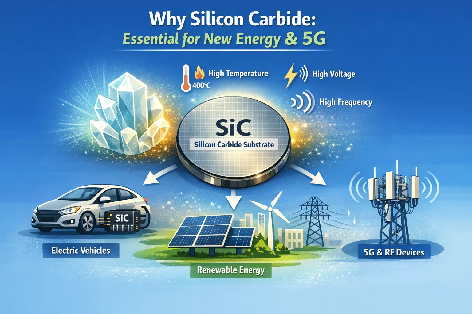
炭化ケイ素基板が新エネルギーと5Gの「必須素材」になった理由
1.はじめにシリコンの限界からワイドバンドギャップのブレークスルーへ 世界の産業が電化とデジタル化に向けて加速する中、従来のシリコン(Si)ベースの半導体は物理的な限界に近づきつつある。

1.はじめにシリコンの限界からワイドバンドギャップのブレークスルーへ 世界の産業が電化とデジタル化に向けて加速する中、従来のシリコン(Si)ベースの半導体は物理的な限界に近づきつつある。
Sapphire substrates, particularly 8-inch wafers, are becoming a critical material in the semiconductor industry. With exceptional mechanical strength, optical transparency, and thermal stability, 8-inch sapphire
Virtual Reality has advanced fast—higher pixel densities, wider fields of view, lighter optics. Yet one part of the device rarely gets the spotlight: the protective