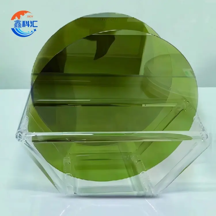
상용 SiC 전력 디바이스가 n형 기판을 사용하는 이유
실리콘 카바이드(SiC)는 전력 전자 분야의 판도를 바꾸는 재료로 부상했습니다. 높은 항복 전압과 뛰어난 열 전도성, 그리고

실리콘 카바이드(SiC)는 전력 전자 분야의 판도를 바꾸는 재료로 부상했습니다. 높은 항복 전압과 뛰어난 열 전도성, 그리고

Silicon carbide (SiC) has rapidly moved from a niche material known only to semiconductor experts to a headline technology powering electric vehicles, renewable energy systems,
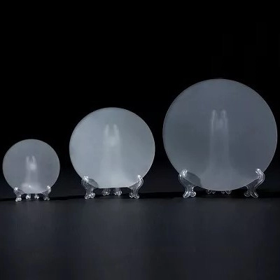
실리콘 카바이드(SiC) 에피택시는 오늘날의 고전압, 고주파, 고효율 반도체 디바이스의 가장 중요한 공정 중 하나입니다. 이 얇은 결정층은
인공 지능은 흔히 알고리즘, GPU, 신경망, 방대한 데이터 세트와 연관되어 있습니다. 하지만 컴퓨터 비전, 로봇 공학, 자율 주행, 첨단 디스플레이의 혁신 뒤에는 인공지능이 있습니다,
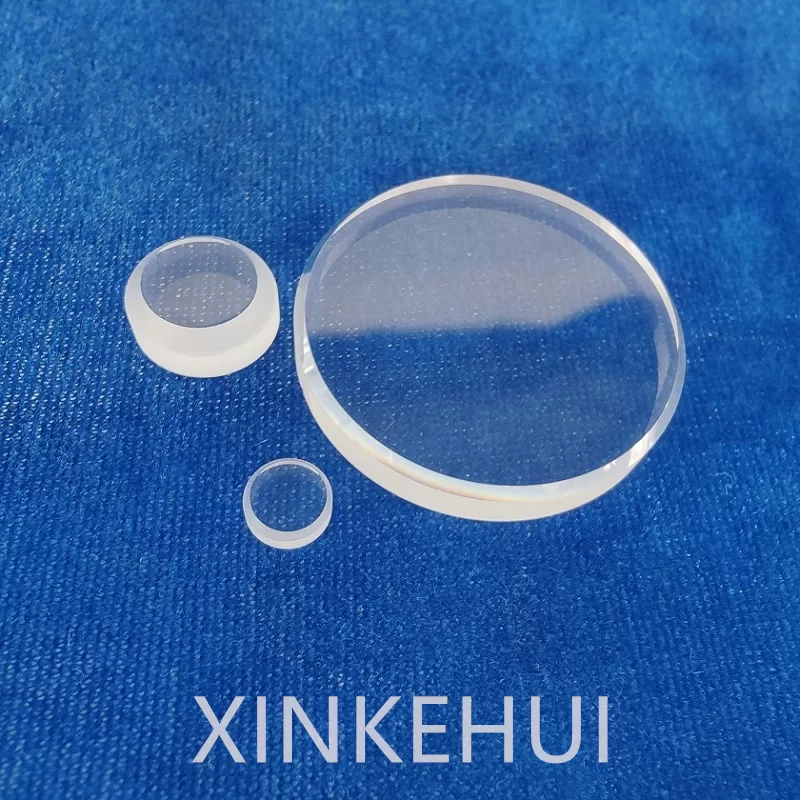
Virtual Reality has advanced fast—higher pixel densities, wider fields of view, lighter optics. Yet one part of the device rarely gets the spotlight: the protective
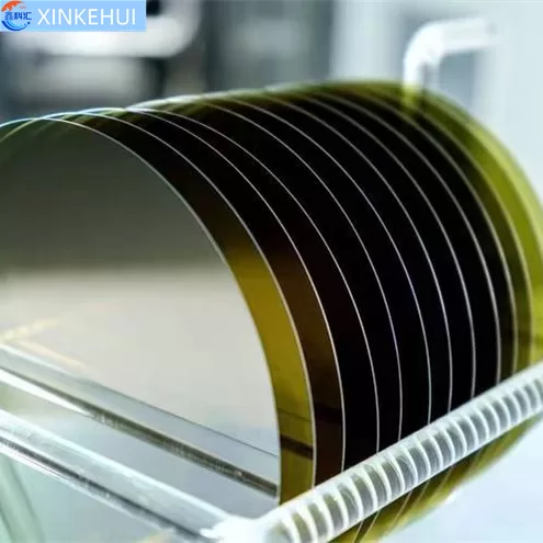
The global shift toward electrification, renewable energy, and high-efficiency power electronics has brought silicon carbide (SiC) wafers into the spotlight. While SiC crystal growth and
When people imagine cutting-edge technology, they think of sleek phones, autonomous vehicles, robots, or AI data centers. Yet almost no one thinks about the thin,