
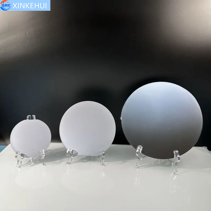
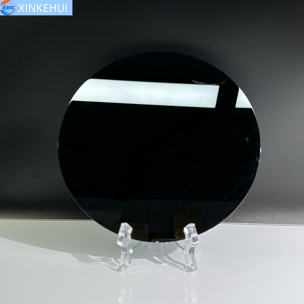
12inch 300mm Silicon wafer’s abstract
A 12-inch (300mm) silicon wafer is a foundational substrate in the semiconductor industry, characterized by its large size and technological significance. These wafers serve as the base material for manufacturing integrated circuits (ICs) and other microelectronic devices due to their superior mechanical, electrical, and thermal properties.In summary, the 12-inch (300mm) silicon wafer stands at the forefront of semiconductor technology, enabling the production of increasingly complex and efficient electronic devices. Its size, material properties, and manufacturing precision make it indispensable in advancing technological innovation across multiple industries.
In summary, the 12-inch 300mm Silicon wafer stands at the forefront of semiconductor technology, enabling the production of increasingly complex and efficient electronic devices. Its size, material properties, and manufacturing precision make it indispensable in advancing technological innovation across multiple industries.
12inch 300mm Silicon wafer’s properties
물리적 속성:
- 지름: 300mm (12 inches)
- Thickness: Typically around 775µm (micrometers), though this can vary slightly based on specific manufacturing requirements.
- Weight: Approximately 100 grams.
기계적 속성:
- 경도: Silicon is a hard and brittle material, with a Mohs hardness of about 7.
- Young’s Modulus: Approximately 130-185 GPa, indicating the stiffness of the300mm Silicon wafer
- Fracture Toughness: Silicon has a low fracture toughness, which means it is prone to cracking under stress.
열 속성:
- 열 전도성: Around 149 W/m·K at 300K, which is relatively high and beneficial for dissipating heat generated in electronic devices.
- Thermal Expansion Coefficient: Approximately 2.6 x 10^-6 /K, indicating how much the wafer will expand with temperature changes.
전기적 속성:
- Band Gap: Silicon has an indirect band gap of about 1.1 eV at room temperature, which is suitable for creating electronic devices like transistors.
- Resistivity: Varies depending on doping; intrinsic silicon has a high resistivity (~10^3 Ω·cm), while doped silicon can have resistivities ranging from 10^-3 to 10^3 Ω·cm.
- Dielectric Constant: Around 11.7 at 1 MHz, which affects the capacitance of devices made from silicon.
Chemical Properties:
- 화학적 안정성: Silicon is chemically stable and resistant to most acids and alkalis at room temperature, except for hydrofluoric acid (HF).
- Oxidation: Silicon forms a native oxide layer (SiO2) when exposed to oxygen at elevated temperatures, which is utilized in semiconductor device fabrication for insulating and protective layers.
Surface Properties:
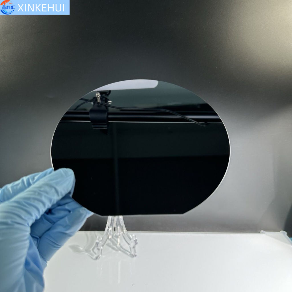
- 표면 거칠기: The surface of a 12-inch 300mm Silicon wafer is polished to a very high degree of smoothness, typically with a surface roughness (Ra) of less than 1 nanometer.
- Flatness: 300mm Silicon wafers are manufactured to be extremely flat, with total thickness variation (TTV) and bow typically less than a few micrometers across the entire wafer.
결정 구조:
- 크리스탈 방향: Common orientations for 300mm Silicon wafer include <100>, <110>, and <111>, each offering different electronic properties and advantages for various applications.
- Lattice Constant: The lattice constant of silicon is about 5.431 Å (angstroms), which defines the repeating distance between atoms in the crystal lattice.
Doping Properties:
- Dopants: 300mm Silicon wafer can be doped with elements such as phosphorus (n-type), boron (p-type), arsenic, and antimony to alter their electrical properties.
- Doping Concentration: Can vary widely depending on the application, from very low concentrations (~10^13 atoms/cm^3) for high-resistivity wafers to very high concentrations (~10^20 atoms/cm^3) for low-resistivity wafers.
The 12-inch 300mm Silicon wafer is a critical component in semiconductor manufacturing due to its excellent physical, thermal, electrical, and chemical properties. Its precise and uniform characteristics make it ideal for producing a wide range of electronic devices, from microprocessors and memory chips to sensors and optoelectronic components.
Usage of 2-inch (50mm) and 12-inch (300mm) Silicon Wafers
1. Integrated Circuits (ICs): Both 2-inch and 12-inch 300mm Silicon wafers are fundamental in the production of integrated circuits. The 12-inch wafers are particularly beneficial for large-scale production due to their ability to accommodate more chips per wafer, significantly reducing manufacturing costs and increasing efficiency.
2. Microelectromechanical Systems (MEMS): MEMS devices, such as accelerometers and gyroscopes, are often fabricated on 2-inch wafers due to their relatively small size and the precision required in their production. However, as MEMS technology advances, larger wafers like the 12-inch ones are increasingly used to scale up production and reduce costs.
3. Power Devices: 300mm Silicon wafers are crucial in manufacturing power devices such as transistors, diodes, and thyristors, which are used in power management systems. The larger 12-inch wafers are advantageous for producing high-power devices due to their ability to handle higher currents and voltages.
4. Photonics and Optoelectronics: In the field of photonics, 300mm Silicon wafers are used to fabricate components like photodetectors, light-emitting diodes (LEDs), and laser diodes. The 2-inch wafers are often used for specialized, high-precision optoelectronic devices, while 12-inch wafers support the mass production of photonic integrated circuits and LED chips.
5. Solar Cells: 300mm Silicon wafers are a key material in the production of photovoltaic cells for solar panels. While 2-inch wafers are typically used for research and development, 12-inch wafers are preferred for commercial solar cell production due to their efficiency in material usage and cost-effectiveness in large-scale manufacturing.
6. Sensors: 300mm Silicon wafers are widely used in manufacturing various sensors, including pressure sensors, temperature sensors, and chemical sensors. The choice between 2-inch and 12-inch wafers depends on the scale of production and the specific application. Smaller 2-inch wafers are often used for high-precision, specialized sensors, while 12-inch wafers are used for large-volume sensor production.
7. Research and Development: In academic and industrial research settings, both 2-inch and 12-inch wafers are used to develop and test new semiconductor technologies. The smaller 2-inch wafers are cost-effective for experimental and prototype development, while the larger 12-inch wafers are used to scale successful technologies for commercial production.
8. Advanced Packaging: 300mm Silicon wafers are used in advanced packaging techniques such as wafer-level packaging (WLP) and through-silicon vias (TSVs), which are essential for modern electronic devices. The larger 12-inch wafers support these advanced packaging methods by providing more surface area for integrating multiple components and interconnects.
결론: Both 2-inch (50mm) and 12-inch 300mm Silicon wafers play critical roles in the semiconductor industry, each serving distinct purposes based on the scale and nature of the application. While 2-inch wafers are commonly used for specialized, high-precision devices and research, 12-inch wafers are preferred for large-scale production, offering significant cost advantages and efficiency in manufacturing a wide range of electronic and optoelectronic devices.
3 types of 12inch 300mm silicon wafers
Three Types of 12-inch (300mm) Silicon Wafers
1. Undoped (Intrinsic) Silicon Wafers:
Description: Undoped300mm Silicon wafers are composed of pure silicon without any intentionally added impurities. These wafers are the foundational material used in various semiconductor processes and research applications.
특성:
- High Resistivity: Due to the absence of dopants, undoped 300mm Silicon wafers have high electrical resistivity, typically in the range of thousands of ohm-centimeters (Ω·cm).
- Low Conductivity: The lack of free carriers (electrons or holes) results in low electrical conductivity.
- 크리스탈 방향: These wafers can be manufactured in different crystal orientations such as <100>, <110>, and <111>, each offering unique properties for different applications.
- 표면 품질: Typically, undoped 300mm Silicon wafers have a highly polished surface to ensure minimal defects and high uniformity, which is crucial for precision applications.
애플리케이션:
- High-Resistivity Applications: Suitable for devices that require minimal interference from electrical conductivity, such as certain types of sensors and detectors.
- Photovoltaic Cells: Used in the production of solar cells, especially in research and development of new solar technologies.
- Research and Development: Provides a pure silicon baseline for experiments and development of new semiconductor processes and materials.
2. Doped Silicon Wafers:
Description: Doped 300mm Silicon wafers have impurities (dopants) added to the silicon to modify its electrical properties. These dopants can be either electron donors or acceptors, creating n-type or p-type silicon, respectively.
Types and Characteristics:
- N-type Doped Wafers:
- Dopants: Common dopants include phosphorus, arsenic, and antimony, which add extra electrons (negative charge carriers) to the silicon lattice.
- 전기적 속성: N-type wafers have higher electrical conductivity due to the presence of free electrons.
- 애플리케이션: Widely used in the fabrication of integrated circuits (ICs), microprocessors, and various power devices where high electron mobility is advantageous.
- P-type Doped Wafers:
- Dopants: Common dopants include boron and gallium, which create “holes” (positive charge carriers) by accepting electrons from the silicon lattice.
- 전기적 속성: P-type wafers have higher electrical conductivity due to the presence of holes.
- 애플리케이션: Essential for complementary metal-oxide-semiconductor (CMOS) technology, sensors, detectors, and various types of transistors.
Doping Concentrations:
- Lightly Doped: Used in applications requiring high resistivity and low free carrier concentration.
- Heavily Doped: Used in applications where low resistivity and high conductivity are needed.
3. Silicon-on-Insulator (SOI) Wafers:
Description: SOI wafers consist of a thin layer of silicon separated from the bulk silicon substrate by an insulating layer, typically silicon dioxide (SiO2). This structure is engineered to enhance performance and efficiency in semiconductor devices.
특성:
- Layered Structure: Comprises a top silicon layer (device layer), an insulating layer (buried oxide layer), and a silicon substrate (handle wafer).
- Reduced Parasitic Capacitance: The insulating layer minimizes parasitic capacitance between the device layer and the substrate, improving speed and efficiency.
- Improved Thermal Performance: The insulating layer helps in reducing thermal conductivity, allowing better heat management in high-power devices.
- Superior Isolation: Provides excellent electrical isolation between devices, which is beneficial for high-density ICs.
애플리케이션:
- Advanced Microprocessors: Utilized in the production of high-performance CPUs and GPUs due to their enhanced speed and reduced power consumption.
- Radio Frequency (RF) Applications: Ideal for RF devices and circuits, as the reduced parasitic capacitance and improved isolation lead to better performance.
- Microelectromechanical Systems (MEMS): Used in MEMS fabrication for their mechanical properties and superior isolation characteristics.
- Optoelectronic Devices: Beneficial in the production of optoelectronic components like photodetectors and LEDs, where reduced capacitance and improved thermal management are critical.
결론: The three main types of 12-inch 300mm Silicon wafers—undoped (intrinsic) silicon wafers, doped silicon wafers (n-type and p-type), and silicon-on-insulator (SOI) wafers—each have distinct properties and advantages tailored to specific applications in the semiconductor industry. From pure research to high-performance electronics and optoelectronics, these wafers play crucial roles in advancing technology and innovation across various fields.
12inch 300mm silicon wafers data chart
Parameter Specification
Diameter 300mm (12 inches)
Thickness 775 ± 15µm
Orientation <100> or <111>
Resistivity 1-10 ohm-cm (or as specified)
Type P-type or N-type
Primary Flat SEMI standard
TTV (Total Thickness Variation) ≤ 2µm
Bow ≤ 40µm
Warp ≤ 40µm
Surface Finish Polished (single or double side)
Particle Count ≤ 50 @ ≥ 0.12µm
Edge Profile Rounded, beveled, or as specified
Crystallographic Orientation Determined by customer requirements
LTV (Local Thickness Variation) ≤ 1µm (in 20mm x 20mm area)
Flatness (GBIR) ≤ 0.5µm (Global Backside Ideal Range)
Polish CMP (Chemical Mechanical Polishing)
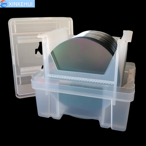
Packaging Cleanroom environment, vacuum-sealed
Q&A
What is the difference between 200mm and 300mm wafers?
The primary differences between 200mm (8-inch) and 300mm (12-inch) wafers lie in their physical dimensions, production efficiencies, and cost implications. Here’s a detailed comparison:
1. Physical Dimensions
- 지름:
- 200mm wafers have a diameter of 200 millimeters (8 inches).
- 300mm wafers have a diameter of 300 millimeters (12 inches).
- 표면적:
- The surface area of a 200mm wafer is approximately 31,400 square millimeters.
- The surface area of a 300mm wafer is approximately 70,685 square millimeters.
2. Production Efficiency
- Chip Yield:
- A 300mm wafer can produce significantly more chips per wafer compared to a 200mm wafer due to the larger surface area. This results in higher production efficiency and lower cost per chip.
- Throughput:
- Larger wafers allow more dies to be fabricated simultaneously, which can increase the throughput of a semiconductor manufacturing process.
3. Cost Implications
- Initial Investment:
- Transitioning from 200mm to 300mm wafer production requires significant capital investment in new equipment and technology upgrades. The equipment for processing 300mm wafers is generally more expensive.
- Cost per Die:
- Despite the higher initial investment, the cost per die is lower with 300mm wafers because the larger wafer size allows for more efficient use of materials and higher yields.
- Operational Costs:
- 300mm wafer fabs tend to have lower operational costs per die due to economies of scale and more advanced automation.
4. Technology and Manufacturing
- Tool Compatibility:
- Equipment and tools designed for 300mm wafers are generally not compatible with 200mm wafers, and vice versa. This includes lithography, etching, and deposition tools.
- 프로세스 복잡성:
- The move to 300mm wafers has often been accompanied by advances in semiconductor process technology, including finer feature sizes and more advanced node processes.
5. Market Adoption
- Industry Trends:
- The semiconductor industry has largely transitioned to 300mm wafers for high-volume production, particularly for advanced nodes and large-scale integration circuits.
- 200mm wafers are still widely used, especially for niche applications, legacy technologies, and certain markets like analog, power devices, and MEMS, where the demand and cost structures differ.
요약
The shift from 200mm to 300mm wafers is driven by the need for greater production efficiency and cost reduction per chip. While the larger 300mm wafers offer significant advantages in terms of chip yield and operational costs, the transition requires substantial initial investment and new infrastructure. The industry trend has been toward adopting 300mm wafers for most advanced semiconductor manufacturing, while 200mm wafers continue to serve specific market needs.
How are 300mm Silicon wafers made into chips?
The process of turning 300mm Silicon wafers into semiconductor chips involves several complex and highly controlled steps. Here is an overview of the key stages:
1. Wafer Preparation
- 크리스탈 성장:
- Pure silicon is melted and a single crystal is grown using the Czochralski process.
- Wafer Slicing:
- The silicon ingot is sliced into thin wafers using a diamond saw.
- 웨이퍼 연마:
- The wafers are polished to a mirror finish to provide a smooth surface for subsequent processing.
- Wafer Cleaning:
- The wafers are thoroughly cleaned to remove any contaminants.
2. Photolithography
- Photoresist Application:
- A light-sensitive material called photoresist is applied to the wafer.
- Mask Alignment and Exposure:
- A mask with the desired circuit pattern is aligned over the wafer. The wafer is then exposed to ultraviolet (UV) light, transferring the pattern onto the photoresist.
- Developing:
- The exposed photoresist is developed, leaving a patterned coating on the wafer.
3. Etching
- Pattern Transfer:
- The wafer is subjected to etching processes (either wet chemical or dry plasma etching) to remove the silicon dioxide or other layers where the photoresist has been removed, creating the circuit patterns in the underlying material.
- Photoresist Removal:
- The remaining photoresist is stripped away.
4. Doping
- Ion Implantation or Diffusion:
- Doping introduces impurities into specific regions of the 300mm Silicon wafer to modify its electrical properties. This can be done through ion implantation or thermal diffusion.
5. Deposition
- Layer Deposition:
- Various thin films of materials (such as silicon dioxide, silicon nitride, or metals) are deposited on the wafer using processes like chemical vapor deposition (CVD) or physical vapor deposition (PVD).
6. Planarization
- Chemical Mechanical Planarization (CMP):
- The wafer surface is planarized to ensure a flat surface for subsequent layers, reducing topographical variations.
7. Metallization
- Interconnect Formation:
- Metal layers are deposited and patterned to form the electrical interconnections between transistors and other components. This usually involves multiple layers of metal separated by insulating layers.
8. Testing and Dicing
- Wafer Testing:
- Electrical tests are performed on each chip (die) on the wafer to ensure they function correctly.
- Dicing:
- The wafer is diced into individual chips using a diamond saw or laser cutting.
9. Packaging
- Chip Mounting:
- Each die is mounted onto a package or substrate.
- Wire Bonding or Flip-Chip:
- Electrical connections are made between the die and the package using wire bonding or flip-chip techniques.
- Encapsulation:
- The chip is encapsulated in a protective plastic or ceramic package to shield it from physical damage and environmental factors.
10. Final Testing
- Functional Testing:
- The packaged chips undergo final testing to ensure they meet all specifications and performance standards.
- 품질 관리:
- Chips that pass testing are marked and sorted for shipment to customers.
요약
The process of making 300mm Silicon wafer into chips involves intricate steps of photolithography, etching, doping, deposition, and metallization, followed by rigorous testing and packaging. Each step must be precisely controlled to produce the high-performance, reliable semiconductor devices used in various electronic applications.