
Siliciumcarbide (SiC) MOSFETs have become essential components in modern power electronics, meeting industry demands for higher efficiency, higher power density, and reliable operation under extreme temperatures. Their applications span electric vehicle (EV) traction inverters, renewable energy systems, industrial power supplies, and high-voltage power modules. The performance of a SiC MOSFET is not only determined by the material properties of SiC but also by the device architecture, which plays a critical role in optimizing conduction, switching speed, and reliability.
SiC offers several inherent advantages over silicon: higher breakdown field strength, higher thermal conductivity, lower on-resistance, faster switching speed, and higher operating temperature. The high breakdown field allows the drift layer to be thinner and more heavily doped, which reduces conduction losses and improves power density, compensating for SiC’s relatively lower channel mobility. Thinner layers also result in smaller junction capacitances, enabling faster switching and higher operating frequencies. Combined, these benefits lead to smaller, lighter, and more efficient power systems.
Below, we detail seven mainstream SiC MOSFET architectures used in industry today.
1. Planar SiC MOSFET
Planar MOSFETs are the first generation of commercial SiC devices and remain widely used due to their mature manufacturing process and high yield. In this architecture, the gate electrode is placed on the SiC wafer surface, forming a horizontal channel.
Voordelen:
- Simple and mature fabrication, lower production costs
- High reliability due to uniform gate oxide on a flat surface
Challenges:
- Longer current paths and JFET effects between cells increase on-resistance
- Limits power density, especially at high operating temperatures
Planar MOSFETs are suitable for cost-sensitive applications where reliability and maturity are prioritized.
2. Trench SiC MOSFET
Trench MOSFETs embed the gate vertically into the SiC substrate, forming a vertical channel along the trench walls. This architecture increases channel density and eliminates the JFET resistance seen in planar devices.
Voordelen:
- Lower on-resistance and improved switching performance
- Higher cell density enables smaller, more efficient chips
Challenges:
- Electric field concentration at the trench bottom may degrade gate oxide reliability over time
- Requires advanced process control to ensure long-term stability
3. Double-Trench SiC MOSFET
The double-trench architecture was introduced to address gate oxide reliability issues in traditional trench designs. ROHM’s third-generation SiC MOSFETs utilize this structure.
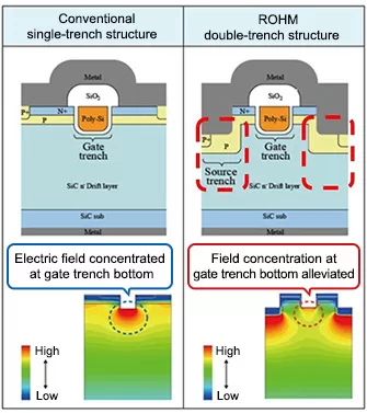
Voordelen:
- Reduced electric field at the trench bottom
- Increased channel density reduces on-resistance by ~50% and lowers input capacitance by ~35%
- Enhanced performance without sacrificing reliability
4. Asymmetric Trench SiC MOSFET
Infineon’s CoolSiC™ series introduced asymmetric trench MOSFETs, where only one side of the trench forms a channel while the other side is optimized for shielding.
Voordelen:
- Balances switching speed and long-term gate oxide reliability
- Reduces gate charge and device capacitance, lowering switching and conduction losses
- Integrated P-shield region supports freewheeling diode performance and eliminates reverse-recovery losses
This architecture is widely deployed in automotive traction inverters and industrial systems, covering voltage ratings from 400 V to 3300 V.
5. Deep Double-Trench and Asymmetric Step-Trench MOSFET
ROHM’s fourth-generation MOSFETs use a deep double-trench (DDT-MOS) design with an extended P-shield and deeper source trenches to reduce gate oxide electric field.
Voordelen:
- Significantly reduces gate oxide stress
- Enhances breakdown voltage while maintaining low on-resistance
Variants:
- The asymmetric step-trench (AST-MOS) combines features of DDT-MOS and Infineon’s asymmetric trench MOSFET (AT-MOS), providing a hybrid solution with improved voltage tolerance and reliability.
6. Trench-Assisted Planar (TAP) MOSFET
Trench-assisted planar architecture represents a compromise between planar and trench designs, employed by GeneSiC Semiconductor.
Voordelen:
- Shallow source trenches reduce cell spacing and on-resistance
- Maintains planar gate manufacturing simplicity and reliability
- Multi-step trench profiles enhance current spreading without deep etching or complex processing
7. V-Groove SiC MOSFET
Mitsubishi Electric developed V-groove SiC MOSFETs, where the gate electrode is embedded in a V-shaped groove on the wafer surface.
Voordelen:
- Lower channel resistance and power loss compared to planar MOSFETs
- Integration of Schottky barrier diodes (SBDs) further enhances high-voltage performance and power density
Challenges:
- Requires specialized etching processes
- Demands precise integration for high-voltage modules
Conclusie
The choice of SiC MOSFET architecture depends on application requirements, including voltage rating, efficiency, reliability, and manufacturing considerations. From planar devices for cost-sensitive designs to trench, double-trench, asymmetric, and V-groove structures for high-performance applications, SiC MOSFETs continue to evolve, enabling smaller, faster, and more efficient power electronics.
By understanding the differences among these seven mainstream architectures, engineers and system designers can optimize their power systems for electric vehicles, industrial drives, renewable energy inverters, and high-voltage applications.