
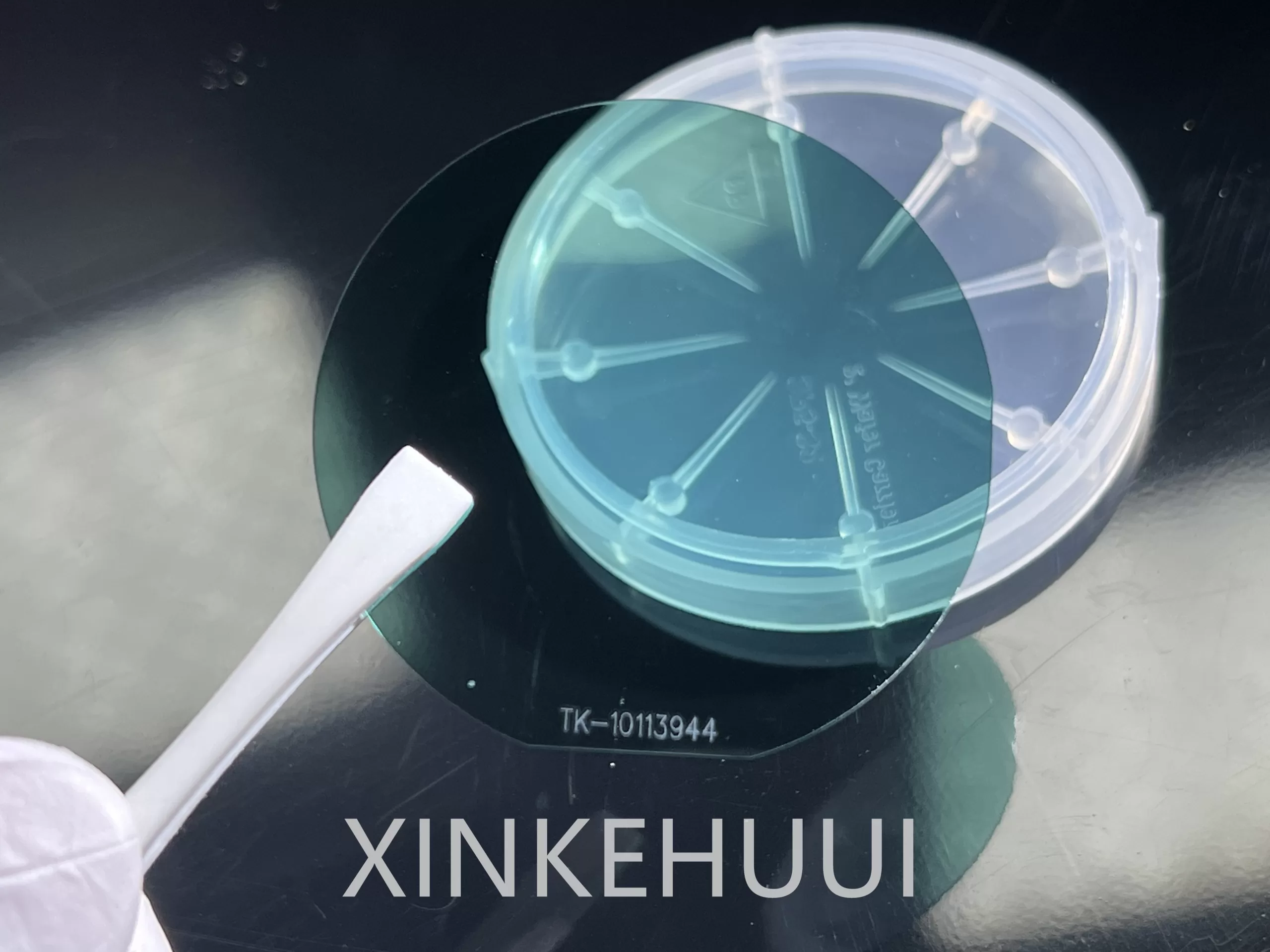
4H-N 4H-Semi SiC substrate’s abstract
4H-N and 4H-Semi SiC substrates are key materials in the field of semiconductor technology, offering unique properties and promising applications. Silicon carbide (SiC) is a wide-bandgap semiconductor material known for its excellent electrical, thermal, and mechanical properties. The 4H crystal structure of SiC provides specific electronic properties suitable for various electronic and optoelectronic devices.
4H-N SiC substrates are typically n-type semiconductors, where nitrogen (N) dopants introduce excess electrons into the crystal lattice, making them suitable for applications requiring electron conduction. These substrates find applications in power electronics, high-frequency devices, and optoelectronics due to their high electron mobility and low on-resistance.
On the other hand, 4H-Semi SiC substrates exhibit semi-insulating behavior, making them ideal for high-power and high-temperature applications. The semi-insulating properties arise from intrinsic defects or intentional doping with deep-level impurities, leading to a high resistivity and minimal electronic conduction. These substrates are widely used in high-power radiofrequency (RF) devices, microwave electronics, and harsh environment sensors.
The fabrication of high-quality 4H-N and 4H-Semi SiC substrates involves advanced growth techniques such as physical vapor transport (PVT), chemical vapor deposition (CVD), or sublimation epitaxy. These techniques enable precise control over the material’s crystal structure, purity, and dopant concentration, resulting in substrates with superior electrical and structural properties.
In recent years, there has been growing interest in utilizing SiC substrates for next-generation electronic and photonic devices. The unique combination of wide-bandgap energy, high breakdown voltage, and thermal stability makes SiC substrates highly desirable for applications in power electronics, RF communications, and photonics. Furthermore, ongoing research aims to optimize the growth processes and material properties of SiC substrates to unlock their full potential in emerging technologies such as quantum computing, high-power lasers, and integrated photonics.
In conclusion, 4H-N and 4H-Semi SiC substrates represent essential building blocks for a wide range of semiconductor devices, offering distinct advantages in terms of electrical performance, thermal management, and reliability. Continued advancements in SiC substrate technology hold great promise for driving innovation in various fields, paving the way for more efficient and robust electronic and optoelectronic systems.
4H-N 4H-Semi SiC substrate’s partial data table
Diameter:2 inches, 3 inches, 4 inches, 6 inches or others
| Grade | Zero MPD Grade | Production Grade | Research Grade | Dummy Grade | |
| Diameter | 150.0 mm +/- 0.2 mm | ||||
| Thickness | 500 um +/- 25 um for 4H-SI350 um +/- 25 um for 4H-N | ||||
| Wafer Orientation | On axis: <0001> +/- 0.5 deg for 4H-SIOff axis: 4.0 deg toward <11-20> +/-0.5 deg for 4H-N | ||||
| Micropipe Density (MPD) | 1 cm-2 | 5 cm-2 | 15 cm-2 | 30 cm-2 | |
| Electrical Resistivity(Ohm-cm) | 4H-N | 0.015~0.025 | |||
| 4H-SI | >1E5 | (90%) >1E5 | |||
| Doping Concentration | N-type: ~ 1E18/cm3SI-type (V-doped): ~ 5E18/cm3 | ||||
| Primary Flat (N type) | {10-10} +/- 5.0 deg | ||||
| Primary Flat Length (N type) | 47.5 mm +/- 2.0 mm | ||||
| Notch (Semi-Insulating type) | Notch | ||||
| Edge exclusion | 3 mm | ||||
| TTV /Bow /Warp | 15um /40um /60um | ||||
| Surface Roughness | Polish Ra 1 nm | ||||
| CMP Ra 0.5 nm on the Si face | |||||
| Cracks by high intensity light | None | None | 1 allowed, 2 mm | Cumulative length 10 mm, single length 2 mm | |
| Hex Plates by high intensity light* | Cumulative area 0.05 % | Cumulative area 0.05 % | Cumulative area 0.05 % | Cumulative area 0.1 % | |
| Polytype Areas by high intensity light* | None | None | Cumulative area 2% | Cumulative area 5% | |
| Scratches by high intensity light** | 3 scratches to 1 x wafer diameter cumulative length | 3 scratches to 1 x wafer diameter cumulative length | 5 scratches to 1 x wafer diameter cumulative length | 5 scratches to 1 x wafer diameter cumulative length | |
| Edge chip | None | 3 allowed, 0.5 mm each | 5 allowed, 1 mm each | ||
| Contamination by high intensity light | None | ||||
4H-N 4H-Semi SiC substrate’s application
- Power Electronics: 4H-N SiC substrates are widely utilized in power electronic devices such as MOSFETs (Metal-Oxide-Semiconductor Field-Effect Transistors), Schottky diodes, and IGBTs (Insulated Gate Bipolar Transistors). Their high electron mobility and low on-resistance make them suitable for high-power and high-frequency applications, including electric vehicles, renewable energy systems, and industrial motor drives.
- RF and Microwave Electronics: Both 4H-N and 4H-Semi SiC substrates find extensive use in radiofrequency (RF) and microwave electronics due to their high breakdown voltage, thermal conductivity, and semi-insulating properties. They are employed in RF power amplifiers, microwave transistors, and high-frequency switches for telecommunications, satellite communications, and radar systems.
- Optoelectronics: SiC substrates are increasingly employed in optoelectronic devices such as UV photodetectors, LEDs (Light-Emitting Diodes), and SiC-based photonic integrated circuits (PICs). The wide bandgap and high thermal conductivity of SiC enable the development of efficient UV detectors and high-brightness LEDs for applications in aerospace, automotive, and medical imaging.
- High-Temperature Electronics: 4H-Semi SiC substrates, with their semi-insulating properties and thermal stability, are well-suited for high-temperature electronics applications. They are utilized in downhole drilling sensors, gas turbine control systems, and aerospace electronics, where traditional silicon-based devices may fail under extreme temperature conditions.
- Harsh Environment Sensors: SiC substrates are ideal for fabricating sensors for harsh environments such as high temperature, radiation, and corrosive atmospheres. They are used in nuclear reactors, chemical processing plants, and space exploration missions for monitoring temperature, pressure, and gas concentrations with high accuracy and reliability.
- Integrated Photonics: Research is ongoing to integrate SiC substrates with photonic devices for applications in integrated photonics and quantum information processing. SiC-based photonic circuits offer advantages such as low optical loss, high power handling, and compatibility with existing semiconductor fabrication processes, enabling the development of advanced optical communication systems and quantum computing technologies.
In summary, 4H-N and 4H-Semi SiC substrates have diverse applications in power electronics (PE), radiofrequency (RF), and microwave (MW) electronics, optoelectronics (OE), high-temperature electronics (HTE), harsh environment sensing (HES), and integrated photonics (IP). Their unique combination of electrical (EL), thermal (TH), and mechanical (ME) properties makes them indispensable for enabling next-generation electronic (E) and photonic (P) systems across various industries.
4H-N 4H-Semi SiC substrate’s properties
- Electrical Properties:
- 4H-N SiC substrates exhibit n-type conductivity due to the presence of nitrogen dopants, providing excess electrons for electronic conduction.
- 4H-Semi SiC substrates demonstrate semi-insulating behavior, characterized by high resistivity and minimal electronic conduction, which is essential for certain electronic and optoelectronic applications.
- Bandgap:
- Both 4H-N and 4H-Semi SiC substrates have a wide bandgap, typically around 3.0 eV for 4H-SiC, enabling their use in high-power and high-frequency devices and optoelectronic applications.
- Thermal Conductivity:
- SiC substrates possess high thermal conductivity, allowing efficient dissipation of heat generated during device operation. This property is crucial for maintaining device reliability and performance, particularly in high-power and high-temperature applications.
- Mechanical Properties:
- SiC substrates exhibit excellent mechanical properties, including high hardness, stiffness, and chemical inertness. These properties make them resistant to mechanical wear and corrosion, ensuring long-term device reliability in harsh operating conditions.
- Crystal Structure:
- Both 4H-N and 4H-Semi SiC substrates have a hexagonal crystal structure (4H polytype), which influences their electronic properties and device performance. The 4H crystal structure provides specific electronic band alignment and carrier mobility suitable for various semiconductor devices.
- Surface Morphology:
- SiC substrates typically have a smooth surface morphology with low defect density, facilitating the growth of high-quality epitaxial layers and the fabrication of high-performance devices.
- Chemical Stability:
- SiC substrates exhibit high chemical stability, making them resistant to degradation when exposed to corrosive environments or reactive chemicals. This property is advantageous for applications requiring long-term device reliability and stability.
- Optical Properties:
- SiC substrates have optical properties that vary with dopant concentration and crystal orientation. These properties are essential for optoelectronic applications such as LEDs, photodetectors, and optical sensors.
In summary, 4H-N and 4H-Semi SiC substrates possess a unique combination of electrical, thermal, mechanical, and optical properties, making them highly suitable for a wide range of electronic and photonic applications in various industries.
Q&A
What is the difference between 4H-SiC and 6H-SiC?
All of the other SiC polytypes are a mixture of the zinc-blende and wurtzite bonding. 4H-SiC consists of an equal number of cubic and hexagonal bonds with a stacking sequences of ABCB. 6H-SiC is composed of two-thirds cubic bonds and one-third hexagonal bonds with a stacking sequences of ABCACB.
What is a SiC substrate?
What are Silicon Carbide (SiC) Wafers & Substrates? Silicon Carbide (SiC) wafers and substrates are specialized materials used in semiconductor technology made from silicon carbide, a compound known for its high thermal conductivity, excellent mechanical strength, and wide bandgap.
A SiC substrate, or silicon carbide substrate, is a crystalline material used as a foundation or base upon which semiconductor devices are fabricated. It is composed of silicon and carbon atoms arranged in a crystal lattice structure, typically exhibiting a hexagonal or cubic crystal structure. SiC substrates are engineered to have specific electrical, thermal, and mechanical properties that make them highly suitable for a wide range of electronic and optoelectronic applications.
SiC substrates offer several advantages over traditional semiconductor materials like silicon (Si), including:
- Wide Bandgap: SiC has a wide bandgap, typically around 2.9 to 3.3 electron volts (eV), which allows for the fabrication of high-power, high-temperature, and high-frequency devices. This wide bandgap enables devices to operate efficiently at higher temperatures and voltages while minimizing leakage current.
- High Thermal Conductivity: SiC substrates have excellent thermal conductivity, which allows for efficient dissipation of heat generated during device operation. This property is critical for maintaining device reliability and performance, especially in high-power and high-temperature applications.
- Chemical Stability: SiC is chemically stable and resistant to corrosion, making it suitable for use in harsh environments and reactive chemical processes. This stability ensures long-term device reliability and stability in various operating conditions.
- Mechanical Hardness: SiC substrates exhibit high mechanical hardness and stiffness, along with resistance to mechanical wear and deformation. These properties contribute to the durability and longevity of devices fabricated on SiC substrates.
- High Breakdown Voltage: SiC devices can withstand higher breakdown voltages compared to silicon-based devices, allowing for the design of more robust and reliable power electronics and high-voltage devices.
- High Electron Mobility: SiC substrates have high electron mobility, which results in faster electron transport and higher switching speeds in electronic devices. This property is advantageous for applications requiring high-frequency operation and fast switching speeds.
Overall, SiC substrates play a crucial role in the development of advanced semiconductor devices for applications in power electronics, radiofrequency (RF) communications, optoelectronics, high-temperature electronics, and harsh environment sensing, among others. Their unique combination of electrical, thermal, and mechanical properties makes them indispensable for enabling next-generation electronic and photonic systems across various industries.