Focus on the field of new material !
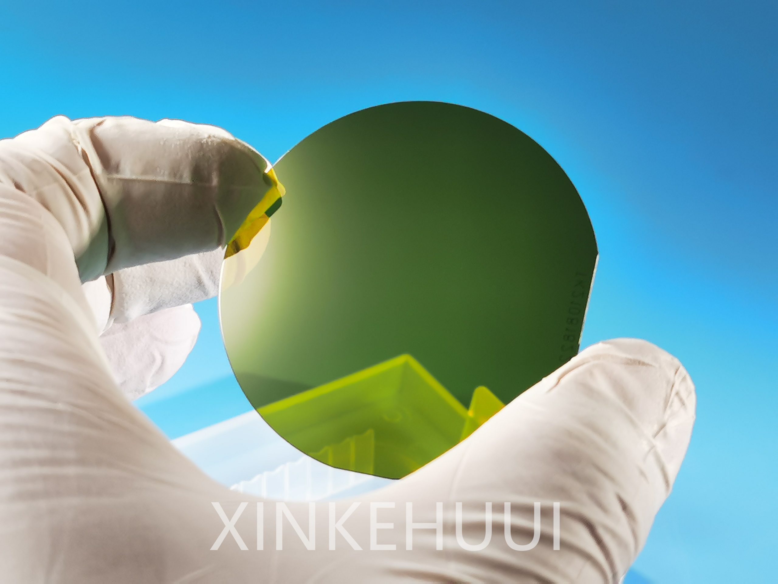

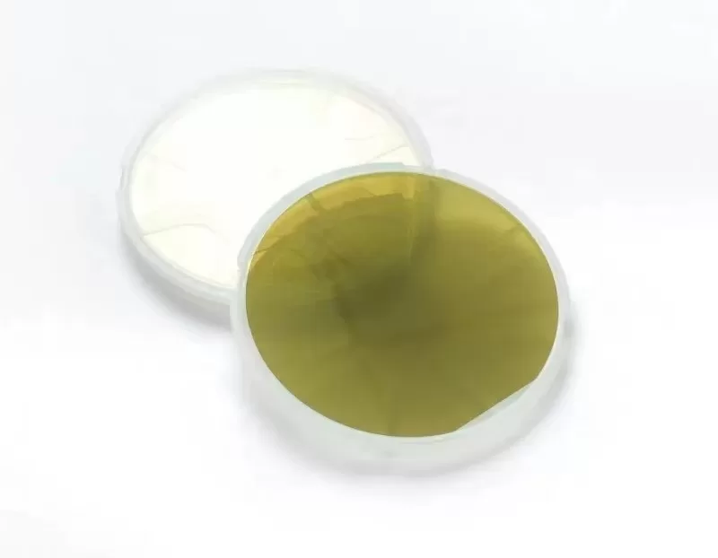
SiC wafer offers a diverse range of Silicon Carbide (SiC) wafers, encompassing five key types: 4H-N, 4H-SEMI, 6H-N, 6H-SEMI, and HPSI. The 4H-N and 6H-N wafers belong to the hexagonal crystal structure, while the 4H-SEMI and 6H-SEMI are specifically tailored for semiconductor applications. HPSI (High Purity Semi Insulating) wafers are designed to meet stringent requirements for applications demanding exceptional purity and insulating properties. These wafers exhibit superior material characteristics, including high thermal conductivity, wide bandgap, and excellent electrical performance, making them ideal for power electronics, RF devices, and high-temperature applications. SICwafer’s commitment to quality ensures that each product adheres to industry standards, providing customers with reliable and cutting-edge solutions for their SiC semiconductor needs.

SiC wafer’s 4H-N Silicon Carbide (SiC) wafers stand out as high-performance semiconductor substrates, showcasing a 4H hexagonal crystal structure. Engineered for electronic applications, these wafers exhibit remarkable electrical properties, making them ideal for power devices and high-frequency applications. The 4H-N SiC wafers offer a wide bandgap, excellent thermal conductivity, and superior electron mobility, ensuring enhanced device performance. With stringent quality control measures in place, SICwafer ensures that each 4H-N SiC wafer meets industry standards, providing reliability for a range of cutting-edge technologies, including power electronics and radio frequency devices. Elevate your semiconductor applications with SICwafer’s precision-engineered 4H-N SiC wafers, delivering advanced solutions for today’s demanding electronic landscape.
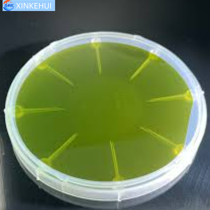
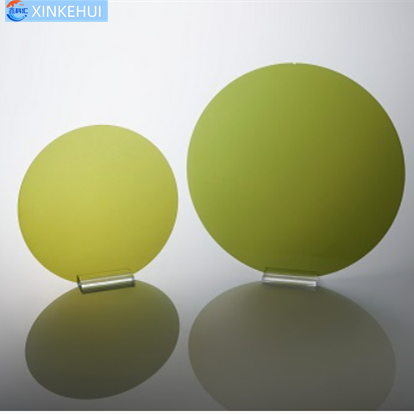
The 6H-N SiC wafer stands at the forefront of semiconductor materials, renowned for its exceptional properties. Characterized by a hexagonal crystal structure, it displays a distinct light yellow to pale blue color, showcasing its unique optical qualities. This wafer excels in electrical conductivity, making it indispensable for high-frequency and high-power electronic devices. With a wide bandgap, it ensures superior performance in demanding conditions. The 6H-N SiC wafer boasts remarkable thermal stability, contributing to efficient heat management across various applications. Its mechanical strength and hardness make it a durable choice for rigorous environments. Widely embraced in the semiconductor industry, this wafer paves the way for cutting-edge electronic components, offering unparalleled innovation and reliability.

The 6H-SEMI SiC wafer stands as a pinnacle in semiconductor materials, featuring exceptional characteristics. With a hexagonal crystal structure, it exhibits distinct properties, including high thermal conductivity and excellent electrical performance. The wafer’s color typically ranges from light yellow to pale blue, a result of its optical nature. Ideal for high-frequency electronic devices, it boasts a wide bandgap, ensuring superior functionality in challenging conditions. The 6H-SEMI SiC wafer excels in thermal stability, vital for efficient heat dissipation. Its mechanical robustness and hardness make it a durable choice for diverse environments. Widely utilized in the semiconductor industry, this wafer facilitates the creation of cutting-edge electronic components, symbolizing innovation and reliability in advanced technology.

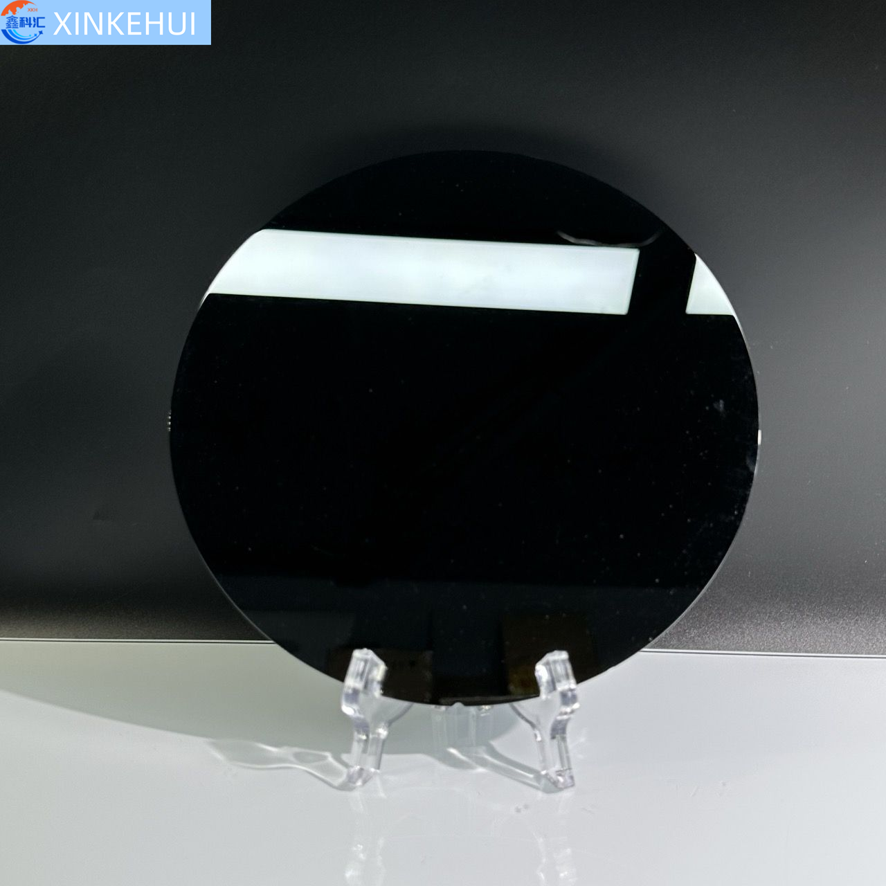
The HPSI SiC wafer represents a high-performance solution in semiconductor materials, known for its outstanding characteristics. With a unique crystal structure, this wafer exhibits excellent thermal conductivity and superior electrical properties. The wafer’s color profile is typically characterized by its distinctive features. Catering to high-frequency electronic devices, it boasts a wide bandgap, ensuring optimal performance in demanding conditions. The HPSI SiC wafer excels in thermal stability, crucial for efficient heat management. Its mechanical strength and hardness make it a durable choice for diverse environments. Widely embraced in the semiconductor industry, this wafer plays a pivotal role in crafting cutting-edge electronic components, epitomizing innovation and reliability in advanced technology.


2inch diameter silicon Carbide(SiC) Substrate Speicfication
| Grade | Zero MPD Grade | Production Grade | Research Grade | Dummy Grade |
| Diameter | 50.6mm±0.2mm | |||
| Thickness | 1000±25um Or other customized thickness | |||
| Wafer Orientation | Off axis : 4.0° toward <1120> ±0.5° for 4H-N/4H-SI On axis : <0001>±0.5° for 6H-N/6H-SI/4H-N/4H-SI | |||
| Micropipe Density | ≤0 cm-2 | ≤2 cm-2 | ≤5 cm-2 | ≤30 cm-2 |
| Resistivity 4H-N | 0.015~0.028 Ω•cm | |||
| Resistivity 4/6H-SI | ≥1E7 Ω·cm | |||
| Primary Flat | {10-10}±5.0° or round shape | |||
| Primary Flat Length | 18.5 mm±2.0 mm or round shape | |||
| Secondary Flat Length | 10.0mm±2.0 mm | |||
| Secondary Flat Orientation | Silicon face up: 90° CW. from Prime flat ±5.0° | |||
| Edge exclusion | 1 mm | |||
| TTV/Bow /Warp | ≤10μm /≤10μm /≤15μm | |||
| Roughness | Polish Ra≤1 nm / CMP Ra≤0.5 nm | |||
| Cracks by high intensity light | None | 1 allowed, ≤2 mm | Cumulative length ≤ 10mm, single length≤2mm | |
| Hex Plates by high intensity light | Cumulative area ≤1% | Cumulative area ≤1% | Cumulative area ≤3% | |
| Polytype Areas by high intensity light | None | Cumulative area ≤2% | Cumulative area ≤5% | |
| Scratches by high intensity light | 3 scratches to 1×wafer diameter cumulative length | 5 scratches to 1×wafer diameter cumulative length | 5 scratches to 1×wafer diameter cumulative length | |
| edge chip | None | 3 allowed, ≤0.5 mm each | 5 allowed, ≤1 mm each | |
| 4H-N Type / High Purity SiC wafer/ingots2 inch 4H N-Type SiC wafer/ingots 3 inch 4H N-Type SiC wafer 4 inch 4H N-Type SiC wafer/ingots 6 inch 4H N-Type SiC wafer/ingots | 4H Semi-insulating / High Purity SiC wafer2 inch 4H Semi-insulating SiC wafer 3 inch 4H Semi-insulating SiC wafer 4 inch 4H Semi-insulating SiC wafer 6 inch 4H Semi-insulating SiC wafer |
| 6H N-Type SiC wafer 2 inch 6H N-Type SiC wafer/ingot | Customzied size for 2-6inch |
The development of Silicon Carbide (SiC) wafers has undergone significant advancements, ushering in a new era in semiconductor technology. SiC wafers have emerged as a key player in the electronics industry due to their unique properties and superior performance compared to traditional silicon wafers. In this comprehensive overview, we will delve into the evolution and progress of SiC wafers, covering their properties, applications, and the impact they have had on various sectors.
Silicon Carbide (SiC) is a compound semiconductor material that has garnered attention for its remarkable electrical, thermal, and mechanical properties. They are thin slices of single crystal SiC used as a substrate for manufacturing electronic devices. The evolution of They has been driven by the quest for materials that can withstand higher temperatures, higher voltages, and offer enhanced power efficiency compared to conventional silicon-based devices.
The evolution of Silicon Carbide (SiC) wafers represents a transformative journey in semiconductor technology. From early explorations to overcoming manufacturing challenges, SiC wafers have emerged as a cornerstone in the development of high-performance electronic devices. Their unique properties have opened up new possibilities in power electronics, automotive, aerospace, and renewable energy. As research and development efforts persist, SiC wafers are poised to play an even more significant role in shaping the future of semiconductor applications.