
Silicon Carbide Wafer’s descriptions
Silicon carbide (SiC), also known as carborundum, represents a versatile semiconductor compound comprised of silicon and carbon with the chemical formula Silicon Carbide Wafer. Renowned for its robustness and resilience, SiC finds widespread utilization in semiconductor electronic devices engineered to operate under extreme conditions characterized by high temperatures, high voltages, or both. SiC extends its applicability beyond semiconductor electronics, emerging as a crucial component within LED technology, where it serves as an optimal substrate for cultivating GaN devices. Moreover, Silicon Carbide Wafer plays a pivotal role as a heat spreader in high-power LED systems, emphasizing its multifaceted significance across diverse technological sectors.
Its exceptional thermal conductivity and superior mechanical properties render SiC indispensable for applications necessitating reliability and performance under demanding environmental conditions. Additionally, SiC exhibits outstanding resistance to chemical degradation, making it an ideal choice for harsh operating environments encountered in various industrial and automotive applications. With ongoing advancements in manufacturing techniques and material properties, SiC continues to drive innovation and enable the development of next-generation electronic and optoelectronic devices, contributing to the advancement of technology and industrial progress.
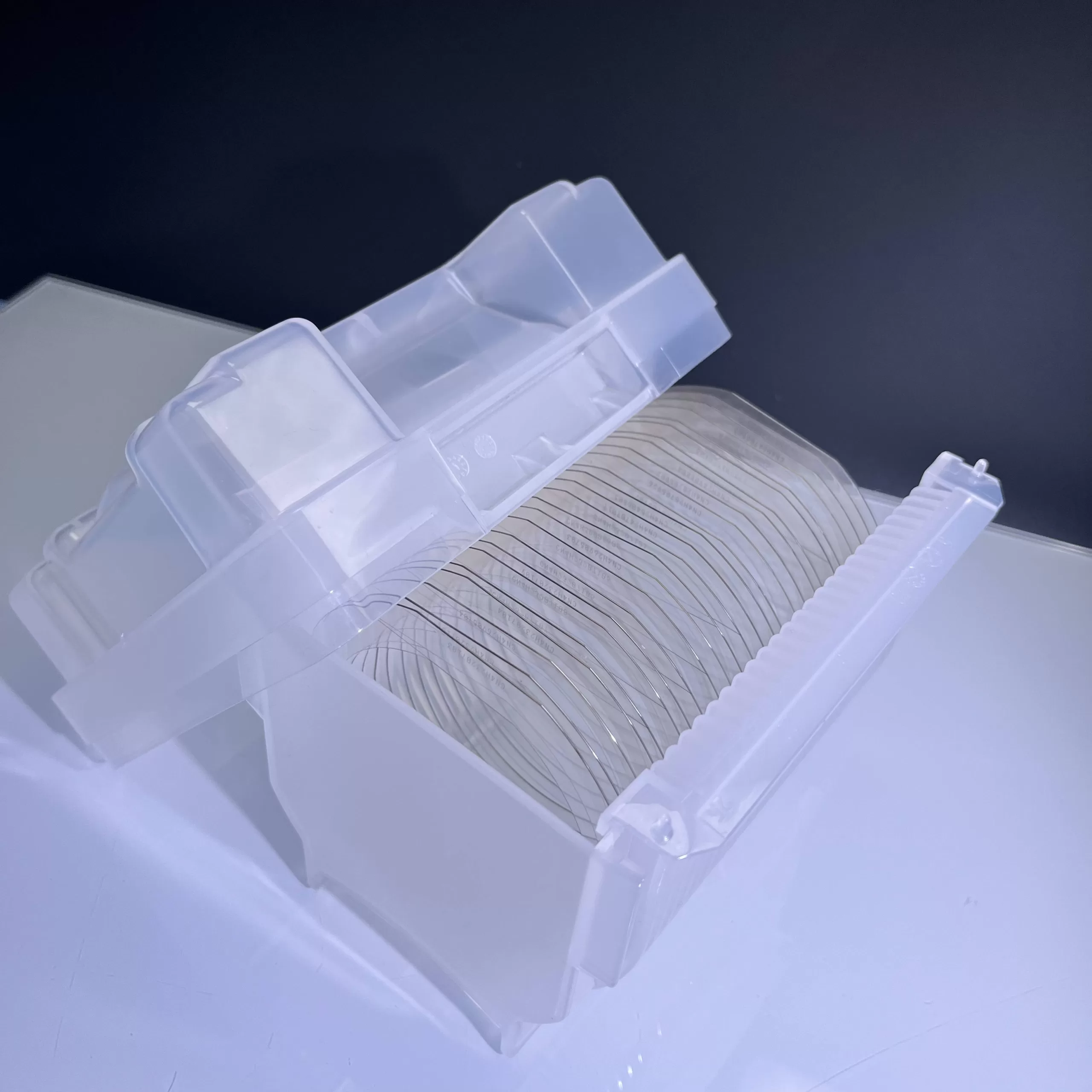
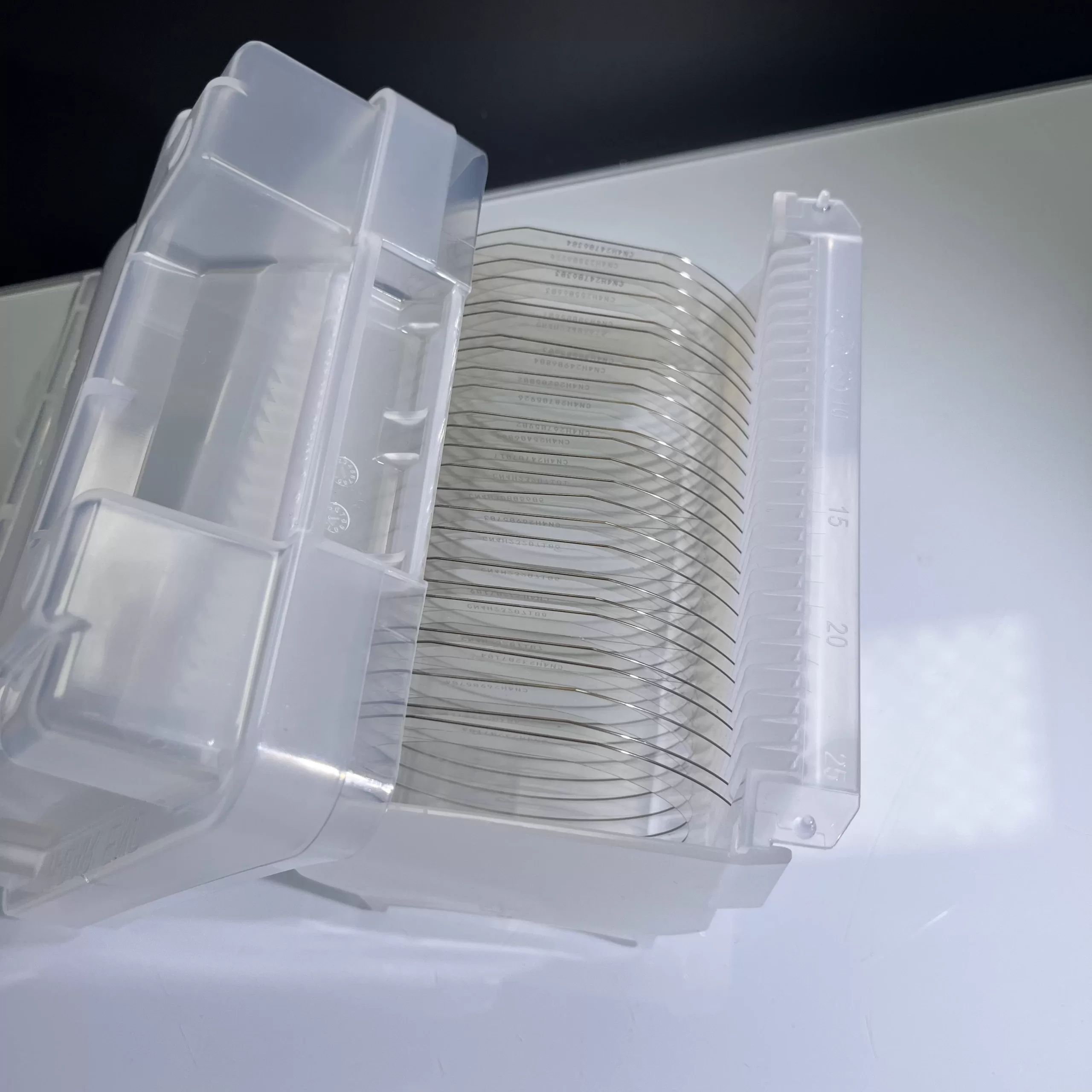
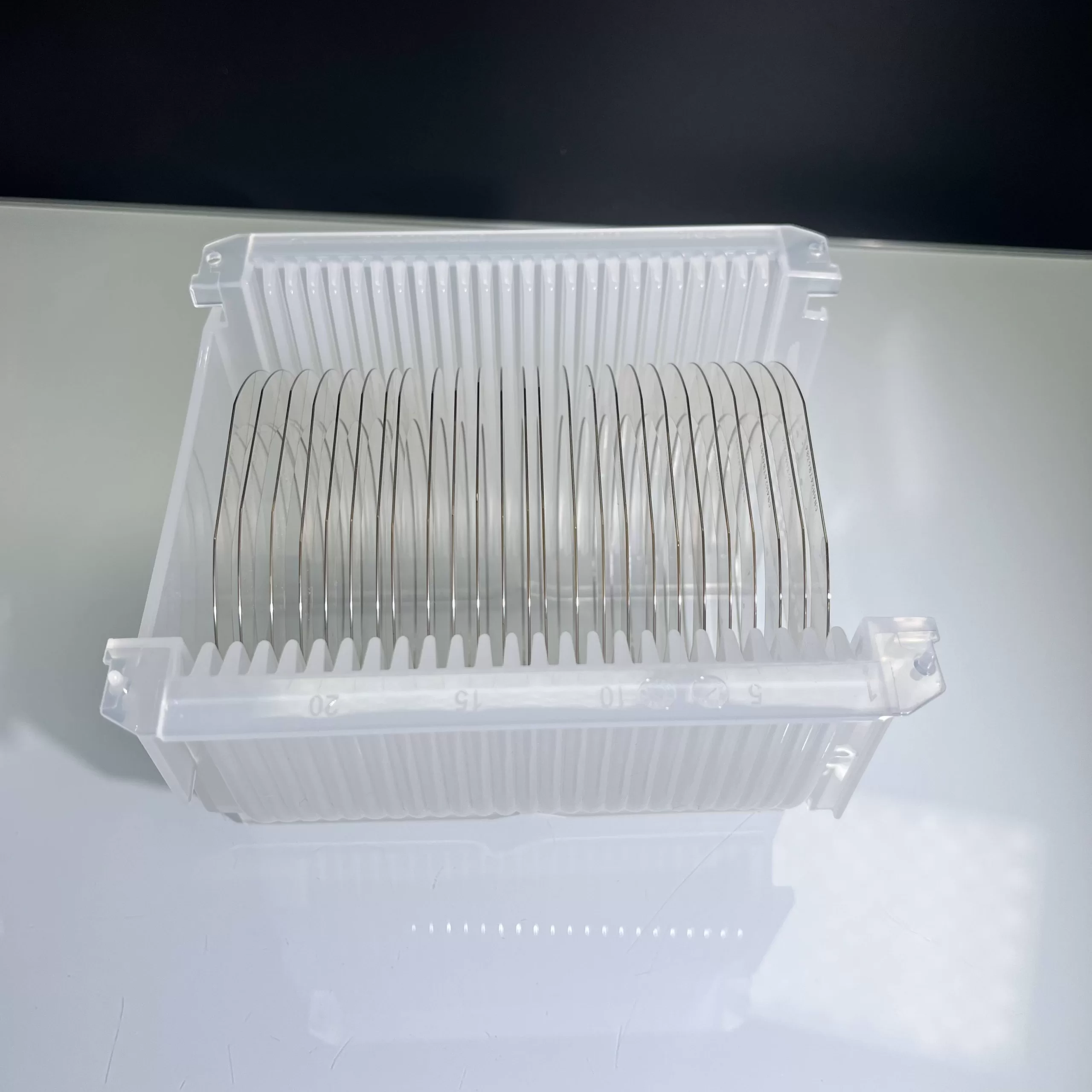
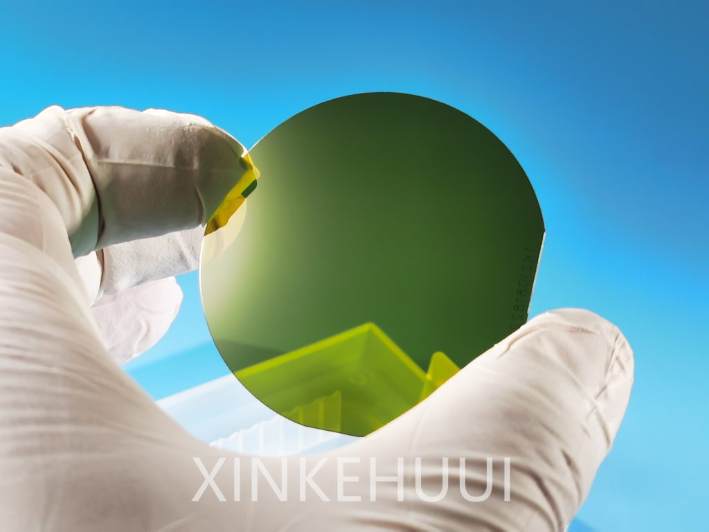
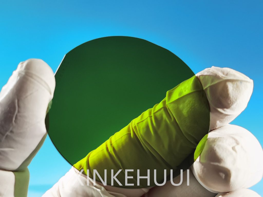
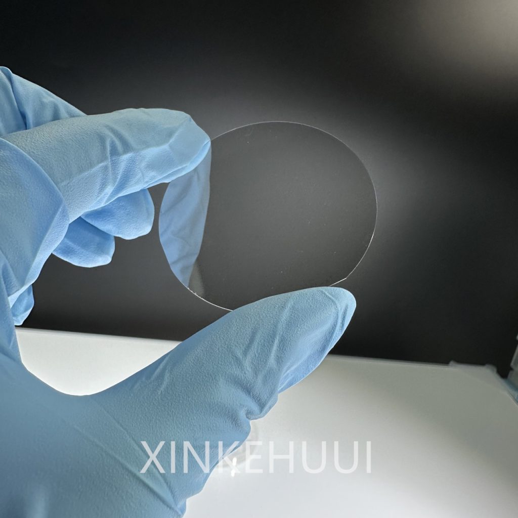
Silicon Carbide Wafer’s shouwcase
Silicon Carbide Wafer’s data sheet(partly)
| Property | 4H-SiC, Single Crystal | 6H-SiC, Single Crystal |
| Lattice Parameters | a=3.076 Å c=10.053 Å | a=3.073 Å c=15.117 Å |
| Stacking Sequence | ABCB | ABCACB |
| Mohs Hardness | ≈9.2 | ≈9.2 |
| Density | 3.21 g/cm3 | 3.21 g/cm3 |
| Therm. Expansion Coefficient | 4-5×10⁻⁶/K | 4-5×10⁻⁶/K |
| Refraction Index @750nm | no = 2.61 ne = 2.66 | no = 2.60 ne = 2.65 |
| Dielectric Constant | c~9.66 | c~9.66 |
| Thermal Conductivity (N-type, 0.02 ohm.cm) | a~4.2 W/cm·K@298K c~3.7 W/cm·K@298K | |
| Thermal Conductivity (Semi-insulating) | a~4.9 W/cm·K@298K c~3.9 W/cm·K@298K | a~4.6 W/cm·K@298K c~3.2 W/cm·K@298K |
| Band-gap | 3.23 eV | 3.02 eV |
| Break-Down Electrical Field | 3-5×10⁶V/cm | 3-5×10⁶V/cm |
| Saturation Drift Velocity | 2.0×10⁵m/s | 2.0×10⁵m/s |
4H-N 4inch diameter Silicon Carbide (SiC) Substrate Specification
2inch diameter Silicon Carbide (SiC) Substrate Specification
| Grade | Zero MPD Grade | Production Grade | Research Grade | Dummy Grade |
| Diameter | 100. mm±0.2mm | |||
| Thickness | 1000±25um Or other customized thickness | |||
| Wafer Orientation | Off axis : 4.0° toward <1120> ±0.5° for 4H-N/4H-SI On axis : <0001>±0.5° for 6H-N/6H-SI/4H-N/4H-SI | |||
| Micropipe Density | ≤0 cm-2 | ≤2 cm-2 | ≤5 cm-2 | ≤30 cm-2 |
| Resistivity 4H-N | 0.015~0.028 Ω•cm | |||
| Resistivity 4/6H-SI | ≥1E7 Ω·cm | |||
| Primary Flat | {10-10}±5.0° or round shape | |||
| Primary Flat Length | 18.5 mm±2.0 mm or round shape | |||
| Secondary Flat Length | 10.0mm±2.0 mm | |||
| Secondary Flat Orientation | Silicon face up: 90° CW. from Prime flat ±5.0° | |||
| Edge exclusion | 1 mm | |||
| TTV/Bow /Warp | ≤10μm /≤10μm /≤15μm | |||
| Roughness | Polish Ra≤1 nm / CMP Ra≤0.5 nm | |||
| Cracks by high intensity light | None | 1 allowed, ≤2 mm | Cumulative length ≤ 10mm, single length≤2mm | |
| Hex Plates by high intensity light | Cumulative area ≤1% | Cumulative area ≤1% | Cumulative area ≤3% | |
| Polytype Areas by high intensity light | None | Cumulative area ≤2% | Cumulative area ≤5% | |
| Scratches by high intensity light | 3 scratches to 1×wafer diameter cumulative length | 5 scratches to 1×wafer diameter cumulative length | 5 scratches to 1×wafer diameter cumulative length | |
| edge chip | None | 3 allowed, ≤0.5 mm each | 5 allowed, ≤1 mm each | |
Silicon Carbide Wafer’s applications
Silicon carbide (SiC) wafers find extensive applications across various industries and technological domains due to their unique properties. Some of the key applications include:
- Power Electronics: Silicon Carbide Wafer are widely used in power electronics applications due to their high breakdown voltage, high thermal conductivity, and low on-resistance. They are employed in devices such as Schottky diodes, MOSFETs, and power modules for efficient power conversion and management.
- High-Temperature Electronics: Silicon Carbide Wafer’s ability to operate at high temperatures makes it suitable for applications in harsh environments, such as aerospace, automotive, and industrial sectors. SiC-based electronics can withstand elevated temperatures without degradation, making them ideal for engine control systems, sensors, and actuators.
- RF and Microwave Devices: Silicon Carbide Wafer wafers are utilized in radio frequency (RF) and microwave devices due to their high electron mobility and low parasitic capacitance. They are employed in applications such as radar systems, communication equipment, and wireless infrastructure for high-frequency operation and low signal loss.
- Optoelectronics: SiC wafers serve as substrates for the growth of gallium nitride (GaN) layers in light-emitting diodes (LEDs) and laser diodes. They provide a stable and lattice-matched platform for GaN epitaxy, enabling the production of high-performance LEDs for lighting, displays, and solid-state lighting applications.
- Automotive Electronics: SiC wafers are increasingly used in automotive electronics for electric vehicle (EV) powertrain components, including inverters, onboard chargers, and DC-DC converters. SiC-based power modules offer higher efficiency, reduced size, and enhanced thermal management compared to traditional silicon-based solutions, contributing to the advancement of electric vehicle technology.
- Renewable Energy: SiC wafers play a crucial role in renewable energy applications, such as solar inverters and wind power converters. Their high-temperature operation capability and high-frequency switching capability enable efficient power conversion and grid integration in renewable energy systems, improving overall energy efficiency and reliability.
- Defense and Aerospace: SiC wafers are utilized in defense and aerospace applications for their ruggedness, reliability, and radiation resistance. They are employed in electronic warfare systems, avionics, and satellite communication systems where performance under harsh environmental conditions is essential.
- Medical Devices: SiC wafers find niche applications in medical devices, particularly in high-temperature sensors, implantable electronics, and biomedical imaging equipment. Their biocompatibility and resistance to chemical corrosion make them suitable for medical applications requiring long-term reliability and durability.
Overall, the versatile properties of SiC wafers enable their utilization across a wide range of applications, contributing to advancements in electronics, energy, communications, transportation, and healthcare industries.
Silicon Carbide Wafer’s properties
Silicon carbide (SiC) wafers exhibit a plethora of unique properties that make them highly desirable for various technological applications. Some of the key properties include:
- High Thermal Conductivity: Silicon Carbide Wafer wafers possess excellent thermal conductivity, allowing for efficient heat dissipation and thermal management in electronic devices and high-power applications.
- Wide Bandgap: Silicon Carbide Wafer has a wide bandgap (2.2-3.4 eV depending on polytype), enabling the fabrication of high-performance electronic and optoelectronic devices capable of operating at elevated temperatures and high voltages.
- High Breakdown Field Strength: Silicon Carbide Wafer exhibit a high breakdown electric field strength, making them suitable for high-voltage and power electronics applications, where they can withstand high electric fields without breakdown.
- High Electron Mobility: Silicon Carbide Wafer feature high electron mobility, facilitating the development of high-speed and high-frequency electronic devices for applications such as RF amplifiers, microwave communication systems, and radar systems.
- Chemical and Thermal Stability: Silicon Carbide Wafer demonstrate exceptional chemical and thermal stability, resisting degradation under harsh environmental conditions, including high temperatures, corrosive atmospheres, and radiation exposure.
- Mechanical Hardness: Silicon Carbide Wafers are characterized by their exceptional mechanical hardness, second only to diamond. This property makes them resistant to mechanical wear, abrasion, and damage, ensuring long-term durability in demanding applications.
- Low Power Losses: Silicon Carbide Wafer exhibit low power losses and low switching losses, resulting in higher efficiency and energy savings in power electronics systems, such as inverters, converters, and motor drives.
- Radiation Resistance: SiC wafers possess inherent radiation resistance, making them suitable for use in radiation-rich environments, such as space applications, nuclear power plants, and particle accelerators.
- Wide Temperature Range: Silicon Carbide Wafer can operate over a wide temperature range, from cryogenic temperatures up to several hundred degrees Celsius, making them suitable for applications in extreme temperature environments.
- Piezoelectric Properties: Certain polytypes of Silicon Carbide Wafer exhibit piezoelectric properties, allowing for the development of sensors, actuators, and transducers for pressure sensing, vibration detection, and energy harvesting applications.
- Optical Transparency: SiC wafers exhibit optical transparency in the ultraviolet (UV) and visible spectra, making them suitable for optoelectronic devices, such as UV photodetectors, LEDs, and laser diodes.
These properties collectively make SiC wafers highly versatile and enable their utilization in a wide range of applications across industries such as power electronics, automotive, aerospace, telecommunications, renewable energy, and more.
The manufacturing process of silicon carbide wafers
The manufacturing process of silicon carbide (SiC) wafers involves several intricate steps to produce high-quality substrates suitable for various applications. Here is an overview of the typical manufacturing process:
- Raw Material Preparation: The process begins with the selection and preparation of high-purity raw materials, including silicon and carbon sources. These materials are meticulously processed and refined to remove impurities and ensure the desired chemical composition.
- Crystal Growth: Silicon Carbide Wafer crystals are grown using various methods, such as the sublimation method (physical vapor transport), the chemical vapor deposition (CVD) method, or the modified Lely method. In the sublimation method, high-purity SiC powder is heated in a furnace under controlled conditions, and SiC crystals gradually form on a seed crystal. The CVD method involves the deposition of SiC layers onto a substrate using precursors in a gas-phase reaction.
- Ingot Formation: The grown SiC crystals are then processed into ingots or boules through methods like slicing, grinding, and polishing. These ingots serve as the starting material for wafer fabrication.
- Wafer Fabrication: The ingots are sliced into thin wafers using precision sawing techniques. The resulting SiC wafers undergo additional processing steps, including lapping, grinding, and polishing, to achieve the desired surface finish, thickness, and flatness.
- Doping: Depending on the desired electrical properties, dopants may be introduced into the SiC wafers through ion implantation or epitaxial growth techniques. This process modifies the conductivity and performance characteristics of the wafers for specific applications.
- Surface Treatment: The Silicon Carbide Wafer may undergo surface treatments, such as chemical etching or oxidation, to modify surface properties or enhance bonding characteristics for subsequent processing steps.
- Quality Control: Throughout the manufacturing process, rigorous quality control measures are implemented to ensure the dimensional accuracy, chemical purity, and defect-free nature of the SiC wafers. Advanced metrology techniques, including X-ray diffraction, scanning electron microscopy, and optical microscopy, are employed to assess the quality and integrity of the wafers.
- Packaging: The finished SiC wafers are carefully inspected, cleaned, and packaged to protect them from contamination and damage during transportation and storage. Proper packaging ensures the integrity of the wafers until they are ready for further processing or use in semiconductor device fabrication.
Overall, the manufacturing process of SiC wafers demands precision, expertise, and stringent quality control to produce substrates with the desired properties and performance characteristics required for advanced electronic and optoelectronic applications.
Additional Information for our silicon carbide wafers
- 2″ Silicon Carbide (SiC) 6H N-Type Epi-Ready
- Diameter: 2 inches
- Type/Dopant: N/Nitrogen
- Orientation: <0001> +/- 0.5 degree
- Thickness: 330 ± 25 um
- Grade: D Grade, MPDä100 cm-2, RT: 0.02-0.2 Ω·cm
- Polished: Single face polished, Si face epi-ready with CMP
- Surface Roughness: <0.5 nm
- 2″ Silicon Carbide (SiC) 4H N-Type Epi-Ready
- Diameter: 2 inches
- Type/Dopant: N/Nitrogen
- Orientation: <0001> +/- 0.5 degree
- Thickness: 330 ± 25 um
- Grade: D Grade, MPDä100 cm-2, RT: 0.01-0.1 Ω·cm, Bow/Warp/TTV<25um
- Polished: Single face polished, Si face epi-ready with CMP
- Surface Roughness: <0.5 nm
- 3″ Silicon Carbide (SiC) 4H N-Type
- Diameter: 3 inches
- Type/Dopant: N/Nitrogen
- Orientation: 4 degree +/- 0.5 degree
- Thickness: 350 ± 25 um
- Grade: D Grade, MPDä100 cm-2, RT: 0.01-0.1Ω·cm, Bow/Warp/TTV<35um
- Polished: Double face polished, Si face epi-ready with CMP
- Surface Roughness: <0.5 nm
- 3″ 4H SI
- Diameter: 3 inches
- Type/Dopant: Semi-insulating/V
- Orientation: <0001> +/- 0.5 degree
- Thickness: 350 ± 25 um
- Grade: D Grade, MPDä100 cm-2, RT: 70% ≥1E5 Ω·cm
- Polished: Double face polished, Si face epi-ready with CMP
- Surface Roughness: <0.5 nm
- 2″ Semi Insulation Silicon Carbide 6H
- Diameter: 2 inches
- Type/Dopant: Semi-insulating/V
- Orientation: <0001> +/- 0.5 degree
- Thickness: 330 ± 25 um
- Grade: D Grade, MPDä100 cm-2, RT: 70% ≥1E5 Ω·cm
- Polished: Single face polished, Si face epi-ready with CMP
- Surface Roughness: <0.5 nm
- 4″ N-type Silicon Carbide (SiC) 4H
- Diameter: 4 inches
- Type/Dopant: N/Nitrogen
- Orientation: 4.0° +/- 0.5°
- Thickness: 350μm ± 25μm
- Grade: D Grade, MPDä100 cm-2, 0.01~0.1Ω•cm, TTV/Bow /Warp<45um
These wafers offer high-quality materials with precise specifications, suitable for various semiconductor and electronic applications.
Q&A
Difference Between Prime and Research Grade Silicon Carbide Wafers?
The difference of Prime grade and Research grade SiC:
- “Prime grade” with useable area>/=90%,defect density i.s MPD</=5/cm^2,resistivity uniformity >/=90%, best “thickness, warp & bow” value, No Surface defects
- “Research grade” with useable area>/=80%,defect density i.s MPD</=10/cm^2, resistivity uniformity >/=80%, better “thickness, warp & bow” value, Very few and small Surface defects
What is a silicon carbide wafer?
What are Silicon Carbide (SiC) Wafers & Substrates? Silicon Carbide (SiC) wafers and substrates are specialized materials used in semiconductor technology made from silicon carbide, a compound known for its high thermal conductivity, excellent mechanical strength, and wide bandgap.
A silicon carbide wafer is a thin slice or disc made from silicon carbide (SiC) material. It is a key component in various semiconductor devices and electronic applications. Silicon carbide wafers are highly desirable due to their exceptional properties, including high thermal conductivity, high breakdown voltage, wide bandgap, and resistance to high temperatures and harsh environments. These wafers are commonly used in power electronics, LED lighting, high-temperature applications, and other advanced semiconductor devices.
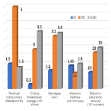
What is the difference between SiC and Si semiconductors?
SiC and GaN materials have a much higher critical breakdown voltage than Si, allowing for a thinner drift layer and higher doping concentration. This leads to lower on-resistance for a given die area and voltage rating, providing for greater efficiency through reduced power loss.
- Material Composition:
- Silicon (Si): Silicon is a widely used semiconductor material with a crystalline structure. It is abundant in nature and has been the dominant material in semiconductor manufacturing for decades.
- Silicon Carbide (SiC): SiC is a compound semiconductor made of silicon and carbon. It is synthesized through a process called the Acheson process or by chemical vapor deposition (CVD). SiC has a crystalline structure similar to diamond.
- Bandgap:
- Silicon (Si): Si has an indirect bandgap, meaning that the minimum energy required for an electron to move from the valence band to the conduction band is higher. This makes Si less efficient for high-power and high-temperature applications.
- Silicon Carbide (SiC): SiC has a wider bandgap compared to Si, making it a wide-bandgap semiconductor. This allows SiC devices to operate at higher temperatures and handle higher voltages with lower losses, making them suitable for high-power and high-frequency applications.
- Thermal Conductivity:
- Silicon (Si): Si has moderate thermal conductivity, which limits its performance in high-temperature applications.
- Silicon Carbide (SiC): SiC has excellent thermal conductivity, even at high temperatures. This property enables SiC devices to dissipate heat more efficiently, making them suitable for applications where thermal management is critical.
- Breakdown Voltage:
- Silicon (Si): Si devices typically have lower breakdown voltages compared to SiC devices.
- Silicon Carbide (SiC): SiC devices can withstand higher breakdown voltages, making them suitable for high-power and high-voltage applications such as power electronics and electric vehicles.
- Switching Speed:
- Silicon (Si): Si devices have lower electron mobility compared to SiC devices, resulting in slower switching speeds.
- Silicon Carbide (SiC): SiC devices have higher electron mobility, allowing for faster switching speeds and reduced switching losses, making them suitable for high-frequency and high-power applications.
In summary, while both Si and SiC are semiconductors used in electronic applications, SiC offers advantages such as higher thermal conductivity, wider bandgap, and higher breakdown voltages, making it particularly suitable for high-power, high-temperature, and high-frequency applications.
Recommendations for Similar Products
SiC substrate used in optoelectronics 4H-N 4H-Semi 350um 500um THE BEST semiconductor material
4H-N and 4H-Semi SiC substrates are key materials in the field of semiconductor technology, offering unique properties and promising applications. Silicon carbide (SiC) is a wide-bandgap semiconductor material known for its excellent electrical, thermal, and mechanical properties. The 4H crystal structure of SiC provides specific electronic properties suitable for various electronic and optoelectronic devices.