Silicon-On-Insulator (SOI) wafers offer a revolutionary platform for semiconductor device fabrication, featuring a thin layer of silicon atop an insulating substrate. This innovative structure provides enhanced performance, reduced power consumption, and improved radiation tolerance compared to traditional bulk silicon substrates. SOI technology enables the development of advanced integrated circuits, microelectromechanical systems (MEMS), and optoelectronic devices for a wide range of applications, including mobile devices, automotive electronics, and aerospace systems. With its superior electrical properties, SOI wafers are driving innovation in the semiconductor industry, paving the way for next-generation electronics with unparalleled efficiency and functionality.
Silicon-On-Insulator (SOI) Wafer’s data sheet(partly)
Processing Method
SIMOX, BONDING, SIMBOND
Diameter
3, 4, 5, 6, 8, 12 Inches
Front side Finish
Polished
Backside Finish
Ground/Polished or Others
Edge Exclusion
2~5mm or less
Handle Wafer
Crystal & Growth Method
Silicon & CZ or FZ
Substrate Thickness
100μm / 300μm / 400μm / 500μm / 625μm ~ Up
Orientation
<100>, <110>, <111> ± 0.5 degree
Dopant
N(Phos., As, Sb) / P(Boron)
Conductivity type
N / P
Resistivity
0.01~10,000 ohm•cm or Upon request
Primary Flat Length
Semi-std
BOX (Buried Oxide Layer)
Buried Thickness
100 nm to 10μm typical
Growth Type
Thermal Oxide
Formed on
Handle Wafer
Device Layer (Multilayer Available)
Thickness of Top Layer
≥ 20 nm
Crystal Growth Method
CZ or FZ
Orientation
<100>,<110>,<111> ± 0.5 degree
Dopant
N(Phos., As, Sb)/P(Boron)
Conductivity type
N / P
Resistivity
0.001~100 ohm•cm or Upon request
Primary Flat Length
Semi-std
Light Point Defect (LPD)
Optional per customer request
Crack
NONE
Haze
NONE
Voids (> 0.5mm² in size)
NONE
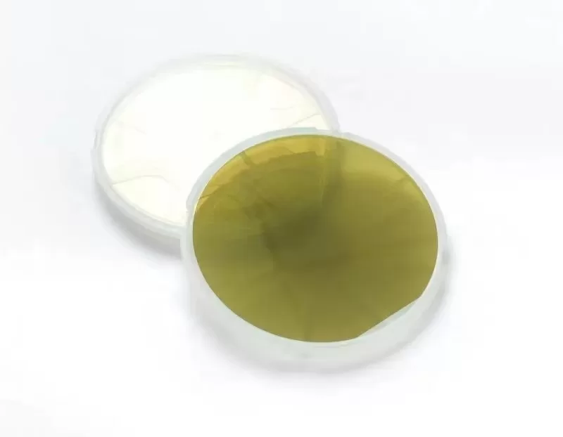
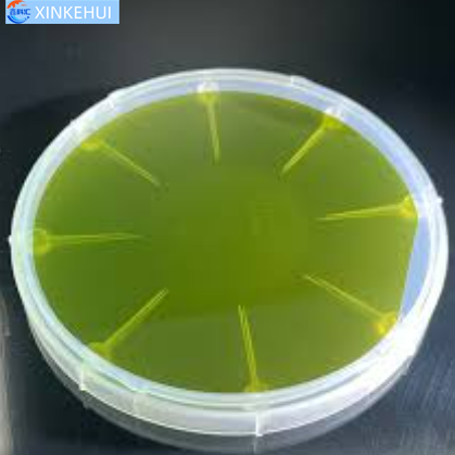
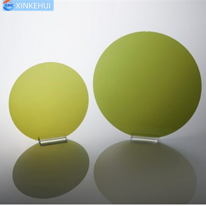
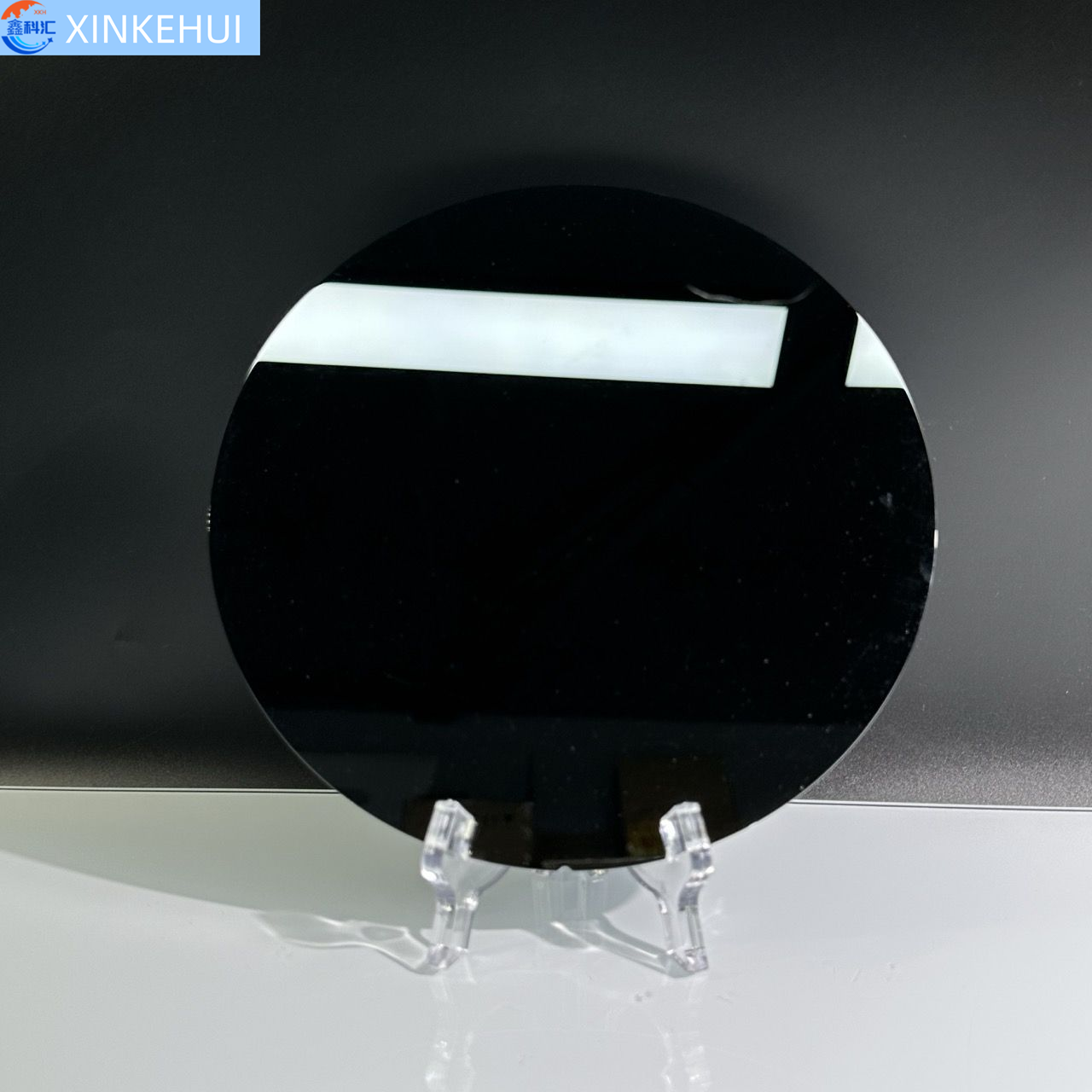
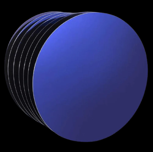
Silicon-On-Insulator (SOI) Wafer’s picture
Silicon-On-Insulator (SOI) Wafer’s applications
Silicon-On-Insulator (SOI) wafers are used in a variety of applications due to their unique properties. Here are some of their main uses:
Microelectronics and Semiconductors: Silicon-On-Insulatorwafers are extensively used in the semiconductor industry for manufacturing various electronic components. They are particularly beneficial for creating high-performance microprocessors, memory chips, and integrated circuits. The SOI technology offers advantages such as reduced parasitic capacitance, lower power consumption, and higher speed compared to traditional silicon wafers.
Radio Frequency (RF) Applications: Silicon-On-Insulator wafers are ideal for RF applications due to their excellent isolation properties. They are used in the fabrication of RF circuits, which are found in wireless communication devices like smartphones, tablets, and GPS devices. The use of SOI technology in these applications can lead to better signal performance and reduced interference.
Photonics: SOI wafers are also used in the field of photonics, including the development of optical components like waveguides, modulators, and photodetectors. The high refractive index contrast between the silicon and the insulator layer allows for tight light confinement, which is beneficial for miniaturizing photonic devices and integrating them with electronic circuits.
MEMS (Micro-Electro-Mechanical Systems): Silicon-On-Insulator wafers provide an excellent platform for MEMS devices, which are used in sensors, actuators, and microsystems. The built-in insulator layer in SOI wafers provides good mechanical and thermal isolation, which is crucial for the performance and reliability of MEMS devices.
Power Devices: Silicon-On-Insulator wafers are used in the manufacturing of power devices, such as power MOSFETs and IGBTs (Insulated Gate Bipolar Transistors). These devices benefit from the SOI structure as it reduces power loss, improves efficiency, and increases the breakdown voltage.
Automotive and Aerospace Electronics: Due to their high performance and reliability, SOI-based devices are increasingly used in automotive and aerospace applications. These environments require components that can withstand high temperatures, vibrations, and radiation levels.
Quantum Computing: Silicon-On-Insulator wafers are being explored as a substrate for quantum computing applications. The insulating layer in Silicon-On-Insulator wafers can be used to isolate and control quantum bits (qubits), which are the basic units of quantum information.
These applications showcase the versatility and importance of Silicon-On-Insulator wafers in the advancement of modern technology across various industries.
Silicon-On-Insulator (SOI) Wafer’s properties
Silicon-On-Insulator (SOI) wafers have several distinctive properties that make them advantageous for various applications in the electronics and photonics industries. Here are some of the key properties:
Reduced Parasitic Capacitance: Silicon-On-Insulator wafers have a lower parasitic capacitance compared to bulk silicon wafers. This results from the insulating layer that separates the silicon active layer from the bulk silicon. Reduced parasitic capacitance leads to faster switching speeds and lower power consumption in electronic devices.
High Electrical Isolation: The buried oxide layer (BOX) in Silicon-On-Insulator wafers provides excellent electrical isolation between the device layer and the substrate. This high isolation is beneficial for reducing leakage currents and crosstalk between devices, which is particularly important in RF and high-speed digital circuits.
Improved Thermal Insulation: The insulating layer in Silicon-On-Insulator wafers also offers better thermal isolation compared to bulk silicon. This property can improve the thermal performance of devices, especially in applications where heat dissipation is critical.
Reduced Short-Channel Effects: Silicon-On-Insulator technology helps in reducing short-channel effects in transistors, which are prevalent as device dimensions shrink. This allows for the creation of smaller devices with higher performance and lower power consumption, extending the scalability of CMOS technology.
Latch-Up Free: Due to the insulating layer, Silicon-On-Insulator devices are immune to latch-up, a problem that can occur in bulk silicon where parasitic thyristor action can lead to device failure.
Higher Breakdown Voltage: Devices built on Silicon-On-Insulator wafers can achieve higher breakdown voltages due to the dielectric isolation provided by the BOX layer. This makes SOI technology suitable for power devices and high-voltage applications.
Better Radiation Hardness: SOI wafers are more resistant to radiation compared to bulk silicon, making them suitable for space and military applications where devices are exposed to high levels of ionizing radiation.
Compatibility with CMOS Processes: Silicon-On-Insulator wafers can be processed using standard CMOS manufacturing techniques, which allows for the integration of SOI-based devices with existing semiconductor manufacturing infrastructure.
Flexibility in Device Design: The properties of SOI wafers allow for a wide range of device structures and types, including fully-depleted and partially-depleted SOI devices. This flexibility enables designers to optimize devices for specific applications.
Low Power Consumption: The combination of reduced leakage currents, lower parasitic capacitance, and reduced short-channel effects leads to significantly lower power consumption in SOI-based devices.
Enhanced Mechanical Stability: The rigid structure provided by the buried oxide layer enhances the mechanical stability of devices, which is beneficial for MEMS and nanoelectromechanical systems (NEMS).
Improved Signal Integrity: For RF and high-speed applications, the improved isolation and reduced parasitic effects in SOI wafers lead to better signal integrity and performance.
These properties contribute to the growing popularity of SOI technology across various sectors, including telecommunications, computing, automotive, and aerospace industries.
The production process of Silicon-On-Insulator (SOI) wafers
The production process of Silicon-On-Insulator (SOI) wafers involves several complex and high-precision steps. Here is a detailed overview of the typical SOI wafer manufacturing process:
Starting Material Preparation: The process begins with high-purity silicon ingots, which are the starting material for most semiconductor devices. These ingots are produced using methods like the Czochralski (CZ) process, where silicon is crystalized from a melt.
Wafer Slicing: The silicon ingots are sliced into thin, flat discs called wafers using a diamond saw. This process must be precisely controlled to ensure that the wafers are of uniform thickness and free of any significant defects.
Wafer Polishing: After slicing, the wafers undergo a series of polishing steps to remove saw marks and surface imperfections. Chemical Mechanical Planarization (CMP) is a common technique used for this purpose, resulting in a mirror-like surface finish.
Oxidation: In the case of the SIMOX (Separation by IMplanted OXygen) method, one of the methods to create SOI structures, the next step involves the implantation of oxygen ions into the silicon wafer. Before this, the wafer surface may be oxidized to form a thin layer of silicon dioxide, which can serve as a marker or barrier during the implantation process.
Oxygen Ion Implantation (for SIMOX): High-energy oxygen ions are implanted into the silicon wafer at a depth that defines the eventual thickness of the silicon layer on top of the insulating layer. The energy and dosage of the implantation process are carefully controlled to achieve the desired depth and concentration of oxygen.
High-Temperature Annealing: After implantation, the wafer is subjected to a high-temperature annealing process, typically above 1300°C. This step allows the oxygen ions to form a continuous layer of silicon dioxide beneath the surface, creating the insulating layer characteristic of SOI wafers.
Bonding (for Bonded SOI): Another common method for SOI production is the wafer bonding technique. In this approach, two silicon wafers are used: one serves as the donor wafer, and the other as the handle wafer. One of the wafers is oxidized to form a silicon dioxide layer, and then the two wafers are brought into contact. The surfaces are treated to promote bonding, and the pair is annealed at high temperatures to strengthen the bond.
Layer Thinning (for Bonded SOI): After bonding, the donor wafer’s thickness is reduced to the desired level, typically using techniques like CMP or etching. This leaves a thin layer of silicon on top of the oxide layer.
Cleaning and Inspection: Following all major processes, the wafers are cleaned to remove any contaminants and inspected for defects. This may involve various cleaning protocols, including wet and dry processes.
Final Inspection and Packaging: The final SOI wafers are thoroughly inspected for any defects, thickness uniformity, and other parameters. Once they pass all quality checks, the wafers are packaged and shipped to customers.
The production of SOI wafers is a highly specialized and technical process, requiring sophisticated equipment and precise control of numerous parameters. The choice of method (e.g., SIMOX, bonded SOI) depends on the application requirements and cost considerations. Each method has its advantages and trade-offs, influencing the final properties and applications of the SOI wafers.
Revolutionizing Industries: Our Diverse Range of SOI Wafers
In the ever-evolving landscape of technology, Silicon-On-Insulator (SOI) wafers stand out as a cornerstone for numerous advanced applications, from microelectronics to photonics. As a leader in the semiconductor industry, [Your Company Name] is proud to offer a wide range of SOI wafers, tailored to meet the innovative demands of modern technology.
Unveiling the Potential of SOI Technology
SOI technology has revolutionized various sectors by providing a platform for high-performance, energy-efficient, and miniaturized devices. The unique structure of an SOI wafer, consisting of a thin layer of silicon separated from the bulk substrate by an insulating layer, offers numerous advantages over traditional silicon wafers. These include reduced parasitic capacitance, minimized power consumption, enhanced speed, and improved thermal performance.
Applications Transformed by SOI Wafers
Our SOI wafers are at the heart of multiple applications across diverse industries:
Microelectronics and Semiconductors: Powering CPUs, memory chips, and advanced integrated circuits, our SOI wafers contribute to faster and more efficient consumer electronics.
Radio Frequency (RF) Devices: In the era of 5G and beyond, our high-resistivity SOI wafers provide superior isolation and performance for RF applications, enabling better connectivity and communication solutions.
Photonics: Our SOI wafers serve as a foundational element for photonic integrated circuits, facilitating advancements in data transmission and optical sensors.
MEMS Devices: From accelerometers to microphones, our wafers offer the ideal substrate for various MEMS applications, ensuring reliability and precision.
Power Electronics: Supporting the development of robust power devices, our SOI wafers aid in achieving higher efficiency and thermal management in power supply systems.
Our Diverse Range of SOI Wafers
At [Your Company Name], we understand that each application has unique requirements. That’s why we offer an extensive selection of SOI wafers, including:
Different Thicknesses and Diameters: Catering to specific design needs, our wafers come in various sizes and thicknesses, ensuring compatibility with different manufacturing processes.
High-Resistivity Wafers: Ideal for RF and high-frequency applications, our high-resistivity wafers minimize parasitic effects and enhance device performance.
Customized SOI Wafers: Beyond our standard offerings, we provide customization options to meet unique specifications, including varied insulator thicknesses, silicon film characteristics, and doping levels.
Commitment to Quality and Innovation
At [Your Company Name], our commitment to excellence is unwavering. We employ stringent quality control measures and state-of-the-art manufacturing processes to ensure that each SOI wafer meets the highest standards. Our dedicated R&D team continuously works on advancing SOI technology, aiming to provide our customers with cutting-edge solutions that drive progress and innovation.
Partnering for Success
We are more than just a supplier; we are a partner in innovation. By choosing [Your Company Name], you gain access to a wealth of knowledge, a broad range of SOI wafer products, and a team committed to your success. Whether you’re at the forefront of microelectronics, paving the way in photonics, or breaking new ground in power electronics, our SOI wafers are here to elevate your projects.
Join the SOI Revolution
As industries continue to evolve, the demand for smaller, faster, and more efficient technologies grows. With [Your Company Name]’s SOI wafers, you are equipped to meet these challenges head-on. Contact us today to discover how our products can revolutionize your applications and lead you to the forefront of innovation.
Q&A
What are SOI wafers?
SOI wafers provide an optimal platform for the manufacture of MEMS, sensor, power and RF devices. Okmetic’s Silicon On Insulator (SOI) wafers are manufactured by bonding technology. Two silicon wafers are bonded together leaving an insulating oxide layer between them.
What is the process of SOI wafer manufacturing?
This process involves the deep implantation of oxygen ions into the surface of a silicon wafer and subsequent annealing at high temperatures. This process produces a thin, uniform silicon layer with low defect density and a sharp Si-SiO2 interface. Additionally, it creates a robust BOX and high carrier mobility.
1. Separation by IMplanted OXygen (SIMOX):
Oxygen Implantation: High-energy oxygen ions are implanted into a silicon wafer at high temperatures. This step involves bombarding the silicon substrate with oxygen ions using an ion implanter.
Annealing: After implantation, the wafer is subjected to a high-temperature annealing process. This step is crucial as it repairs the silicon lattice damage caused by the ion implantation and forms a continuous buried oxide (BOX) layer by allowing the oxygen atoms to diffuse and react with silicon.
Cooling: The wafer is cooled down to room temperature. The result is a structure with a thin silicon layer on top of the insulating oxide layer, separated from the bulk silicon.
2. Wafer Bonding:
Wafer Cleaning: Two silicon wafers are cleaned thoroughly to remove all surface contaminants. This step is critical to ensure the bonding process is successful.
Oxidation: One or both wafers are subjected to thermal oxidation to grow a thin layer of silicon dioxide on their surfaces.
Bonding: The two wafers are brought into contact, with the oxide layers facing each other. The wafers are then bonded together at room temperature due to Van der Waals forces.
High-Temperature Annealing: The bonded wafer pair is annealed at high temperatures, which strengthens the bond between the wafers and removes any existing air bubbles or defects.
Thinning: The top silicon wafer is thinned down to the desired thickness using techniques such as mechanical grinding and chemical-mechanical polishing (CMP).
3. Smart Cut (a variant of the wafer bonding method):
Hydrogen Implantation: Hydrogen ions are implanted into a donor silicon wafer to define the thin layer of silicon that will be transferred.
Wafer Bonding: The donor wafer, with the implanted hydrogen layer, is bonded to a second silicon wafer that has an oxide layer on its surface.
Splitting: The bonded wafers are subjected to a thermal process, where the hydrogen ions expand, creating micro-bubbles that cause the top layer of the donor wafer to split off at the implanted depth.
Final Thinning and Polishing: The transferred silicon layer is then thinned down to the desired thickness and polished to achieve the required surface quality.

 Wafer: Cutting-Edge Technology for High-Performance Electronics 6inch 8inch-Sapphire Wafer_Silicon Wafer_SIC Wafer_GaAs Substrate_ZnSe Windows_Quartz Glass")
 Wafer: Cutting-Edge Technology for High-Performance Electronics 6inch 8inch-Sapphire Wafer_Silicon Wafer_SIC Wafer_GaAs Substrate_ZnSe Windows_Quartz Glass")
 Wafer: Cutting-Edge Technology for High-Performance Electronics 6inch 8inch-Sapphire Wafer_Silicon Wafer_SIC Wafer_GaAs Substrate_ZnSe Windows_Quartz Glass")