
SOI Wafers’ abstract
Silicon-On-Insulator (SOI) wafers have emerged as essential substrates in semiconductor manufacturing, offering unique advantages over traditional silicon substrates. This abstract provides an overview of the composition, fabrication methods, structural properties, electrical characteristics, and diverse applications of SOI wafers, highlighting their significance in advancing semiconductor technology and enabling innovations in electronics, photonics, and beyond.
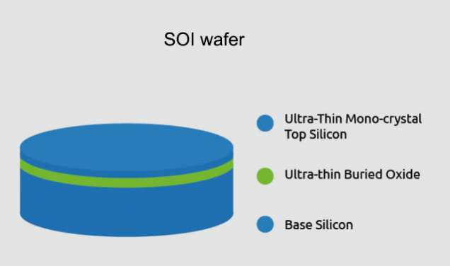
SOI wafers consist of a thin layer of single-crystal silicon (device layer) atop an insulating layer, typically composed of silicon dioxide (SiO2), which is further supported by a silicon substrate (handle wafer). The fabrication of SOI wafers involves advanced techniques such as wafer bonding, ion implantation, and selective etching, resulting in precise control over layer thickness, uniformity, and crystal quality.
The structural properties of SOI wafers, including layer thickness, crystalline quality, and defect density, play a crucial role in determining device performance and reliability. Advanced characterization techniques such as transmission electron microscopy (TEM) and X-ray diffraction (XRD) are employed to assess the quality and integrity of SOI layers for various applications.
SOI wafers offer several key advantages over conventional bulk silicon substrates, including reduced parasitic capacitance, improved device isolation, enhanced radiation hardness, and increased integration density. These advantages stem from the thin buried oxide (BOX) layer that electrically isolates the device layer from the handle wafer, minimizing substrate-related effects and enabling the fabrication of high-performance semiconductor devices.
In terms of electrical characteristics, SOI wafers exhibit superior transistor performance, lower power consumption, and higher operating speeds compared to bulk silicon substrates. The reduced junction capacitance and improved electrostatic control in SOI devices contribute to enhanced device performance, making them ideal for applications requiring high-speed, low-power operation.
SOI wafers find diverse applications across various industries, including microelectronics, telecommunications, photonics, and MEMS/NEMS (microelectromechanical/nanoelectromechanical systems). In microelectronics, SOI technology enables the development of advanced integrated circuits (ICs), system-on-chip (SoC) devices, and radio frequency (RF) components with improved performance and reliability.
In telecommunications and photonics, SOI wafers are utilized for the fabrication of optical modulators, photodetectors, waveguides, and integrated optical circuits. The high optical transparency and low optical loss of SOI substrates make them ideal platforms for implementing silicon photonics solutions for data communication and sensing applications.
In MEMS/NEMS applications, SOI wafers serve as substrates for the fabrication of microelectromechanical and nanoelectromechanical systems, including sensors, actuators, accelerometers, and gyroscopes. The mechanical stability, thermal insulation, and compatibility with standard CMOS (complementary metal-oxide-semiconductor) processes make SOI wafers well-suited for MEMS/NEMS integration with electronics.
In conclusion, SOI wafers represent a significant advancement in semiconductor technology, offering unparalleled performance, integration, and versatility for a wide range of applications. Their unique structural, electrical, and mechanical properties make them indispensable substrates for driving innovations in electronics, photonics, and MEMS/NEMS, paving the way for next-generation semiconductor devices and systems. Continued research and development efforts in SOI technology are expected to further expand its impact and enable transformative advancements in various industries and technological domains.
SOI Wafers’ data chart(Other specifications available for sale.)
| Growth method | Cz, MCz, A-MCz® |
| Diameter | 150 mm, 200 mm |
| Crystal orientation | <100>, <110>,<111> |
| N type dopants | Antimony, Phosphorus |
| P type dopants | Boron |
| Resistivity | From <0.001 to >7,000 Ohm-cm* *Resistivity range varies by dopant and orientation |
| Device layer thickness | From 1 μm to >200 μm Tolerance ±0.5 μm (standard BSOI), ±0.3 μm (0.3 SOI), ±0.1 μm (E-SOI®, Power Management SOI), ±0.5 μm or lower (C-SOI®) |
| Buried oxide layer thickness | From 0.3 μm to 4 μm, typically between 0.5 μm and 2 μm Type: Thermal oxide |
| Handle wafer thickness | 200 mm: 300 μm to 950 μm, typically 725 μm 150 mm: 300 μm to 950 μm, typically 380 μm in 150 mm |
| Back surface | Polished or etched |
| Terrace area | Standard or Terrace Free (Available for 200 mm BSOI, E-SOI® and Power Management SOI) |
SOI Wafers’ applications
Silicon-On-Insulator (SOI) wafers have gained significant attention and adoption across various industries due to their unique properties and versatile applications. Below, we delve into a comprehensive exploration of the diverse applications of SOI wafers across different sectors.
- Semiconductor Industry
- Integrated Circuits (ICs): SOI wafers are extensively utilized in the production of advanced ICs due to their superior electrical properties, such as reduced parasitic capacitance and improved transistor performance. This results in faster switching speeds and lower power consumption, making SOI-based ICs ideal for high-performance computing applications.
- System-on-Chip (SoC) Design: SOI technology enables the integration of multiple functions onto a single chip, facilitating the development of complex SoCs for applications ranging from smartphones and IoT devices to automotive electronics and data centers.
- Radio-Frequency (RF) and Analog Circuits: SOI wafers are preferred for RF and analog circuits due to their low substrate noise, high linearity, and improved isolation, making them suitable for wireless communication systems, RF front-ends, and high-frequency applications.
- Microelectromechanical Systems (MEMS)
- SOI wafers serve as a substrate for the fabrication of MEMS devices, offering excellent mechanical stability, low parasitic capacitance, and high insulation. MEMS applications include accelerometers, gyroscopes, pressure sensors, microphones, and optical switches used in consumer electronics, automotive, healthcare, and industrial sectors.
- Photonics and Optoelectronics
- SOI technology enables the integration of optical components, such as waveguides, modulators, photodetectors, and lasers, with electronic circuits on the same chip. This integration facilitates the development of photonic integrated circuits (PICs) for applications in telecommunications, data communication, sensing, and imaging.
- Power Electronics
- SOI wafers find applications in power electronics due to their high breakdown voltage, low on-resistance, and improved thermal performance. SOI-based power devices, such as insulated gate bipolar transistors (IGBTs) and silicon carbide (SiC) MOSFETs, are used in electric vehicles, renewable energy systems, industrial motor drives, and power supplies.
- Biomedical and Healthcare
- SOI wafers are utilized in biomedical devices and lab-on-chip systems for various applications, including DNA sequencing, drug delivery, biosensing, and medical imaging. The compatibility of SOI with microfluidics and bioMEMS technologies enables the development of miniaturized and portable diagnostic tools with enhanced sensitivity and specificity.
- Sensor Networks and Internet of Things (IoT)
- SOI-based sensors, such as temperature sensors, pressure sensors, and inertial sensors, play a crucial role in IoT applications for monitoring and control in smart homes, smart cities, industrial automation, and environmental sensing. The low-power consumption and small form factor of SOI-based sensors make them suitable for battery-operated and wireless sensor networks.
- Aerospace and Defense
- SOI technology is utilized in aerospace and defense applications for the development of high-performance electronics, radar systems, communication satellites, and unmanned aerial vehicles (UAVs). The radiation hardness and reliability of SOI devices make them well-suited for harsh environments and mission-critical operations.
The realm of Silicon-On-Insulator (SOI) wafers extends far beyond the confines of a singular industry, instead permeating through a multitude of sectors with its versatile applications, igniting a spark of innovation in electronics, photonics, MEMS, biomedical devices, power systems, and beyond. As we embark on a comprehensive exploration of the vast landscape that SOI wafers traverse, we unveil the intricate tapestry of advancements and opportunities that lie ahead.
At the heart of the semiconductor industry, SOI wafers serve as catalysts for revolutionizing Integrated Circuits (ICs), ushering in an era of enhanced performance and efficiency. Through their unique electrical properties, including reduced parasitic capacitance and heightened transistor efficacy, SOI-based ICs propel forward the domains of high-performance computing, enabling faster processing speeds and diminished power consumption. The integration of multiple functions onto a single chip, facilitated by SOI technology, paves the way for the development of intricate System-on-Chip (SoC) designs, catering to an array of applications spanning from handheld devices to sprawling data centers.
Venturing into the realm of Microelectromechanical Systems (MEMS), SOI wafers emerge as the substrate of choice, offering unparalleled mechanical stability and insulation. MEMS devices, ranging from accelerometers to pressure sensors, harness the capabilities of SOI wafers to deliver precision and reliability across diverse sectors, encompassing consumer electronics, automotive technologies, healthcare, and industrial automation.
In the realm of photonics and optoelectronics, the fusion of optical components with electronic circuits on SOI wafers heralds the dawn of a new era in communication and sensing. Photonic Integrated Circuits (PICs), empowered by SOI technology, find applications in telecommunications, data communication, and sensing modalities, promising heightened efficiency and scalability in an increasingly interconnected world.
Power electronics witness a paradigm shift with the integration of SOI wafers, as they bestow upon power devices attributes such as high breakdown voltage and reduced on-resistance. From electric vehicles to renewable energy systems, SOI-based power devices emerge as linchpins in the transition towards sustainable energy solutions, driving innovation and efficiency across the power spectrum.
Biomedical and healthcare sectors witness a convergence of SOI technology with advancements in diagnostics and therapeutic modalities. Lab-on-chip systems and biomedical devices leverage the compatibility of SOI wafers with microfluidics and bioMEMS technologies to deliver portable and precise solutions for disease diagnosis, drug delivery, and medical imaging.
The proliferation of Sensor Networks and Internet of Things (IoT) is propelled by the integration of SOI-based sensors, offering low-power consumption and miniaturization for diverse applications ranging from environmental monitoring to industrial automation. In aerospace and defense, the robustness and reliability of SOI devices find resonance, as they navigate the rigors of mission-critical operations and harsh environments with aplomb.
As we look towards the horizon, the trajectory of SOI technology unveils a landscape rich with promise and potential. Continued advancements in SOI technology are poised to unlock new frontiers in emerging fields such as quantum computing, neuromorphic computing, and beyond-CMOS devices, offering a glimpse into a future shaped by innovation and ingenuity.
In conclusion, the journey of SOI wafers transcends the boundaries of industries, weaving a tapestry of innovation that spans electronics, photonics, MEMS, biomedical devices, power systems, and beyond. As we embark on this odyssey of discovery, the possibilities are boundless, heralding a future shaped by the limitless potential of SOI technology.
SOI Wafers’ properties
Silicon-On-Insulator (SOI) wafers, with their distinctive properties and characteristics, form the bedrock upon which a myriad of technological innovations stand. As we embark on an exploration of these foundational properties, we unravel the intricacies that underpin the versatility and utility of SOI wafers across various industries and applications.
- Insulation Layer Thickness:
- At the heart of SOI wafers lies the insulation layer, which separates the thin layer of silicon from the bulk substrate. The thickness of this insulation layer plays a pivotal role in determining the electrical and mechanical properties of the wafer. Typically ranging from a few nanometers to several micrometers, the insulation layer provides isolation and minimizes parasitic capacitance, thereby enhancing the performance of electronic devices.
- Silicon Layer Thickness:
- The thickness of the silicon layer atop the insulation layer is a critical parameter influencing the performance of SOI wafers. Thinner silicon layers offer improved electrostatic control, reduced short-channel effects, and enhanced transistor performance, making them well-suited for high-speed and low-power applications. Conversely, thicker silicon layers provide mechanical robustness and thermal stability, catering to MEMS and power device applications.
- Crystal Quality:
- The crystalline quality of the silicon layer is paramount in determining the functionality and reliability of devices fabricated on SOI wafers. High-quality crystalline substrates, devoid of defects and dislocations, ensure uniform device performance and yield. Advanced crystal growth techniques, such as epitaxial growth and wafer bonding, are employed to achieve superior crystal quality, thereby enhancing the overall efficiency and reliability of SOI-based devices.
- Substrate Material:
- SOI wafers are typically fabricated on crystalline silicon substrates, although alternative materials such as silicon germanium (SiGe) and sapphire are also utilized for specific applications. The choice of substrate material influences the thermal conductivity, mechanical properties, and compatibility with fabrication processes, thereby shaping the performance and versatility of SOI wafers across diverse industries.
- Thermal Properties:
- Thermal management is paramount in electronic and optoelectronic devices to ensure reliability and performance under varying operating conditions. SOI wafers exhibit excellent thermal properties, including high thermal conductivity and low thermal resistance, facilitating efficient heat dissipation and thermal stability. These properties are particularly advantageous in power electronics, high-power RF devices, and optoelectronic applications.
- Electrical Properties:
- SOI wafers offer unique electrical properties that distinguish them from traditional bulk silicon substrates. Reduced parasitic capacitance, enhanced transistor performance, and improved isolation are among the key electrical advantages conferred by SOI technology. These properties enable the development of high-speed, low-power, and radiation-hardened devices for applications ranging from integrated circuits to sensor networks.
- Mechanical Stability:
- MEMS devices fabricated on SOI wafers benefit from the mechanical stability and flatness of the substrate, which ensure precise operation and reliability. The robustness of SOI wafers against mechanical stresses and strains makes them ideal for MEMS applications requiring high sensitivity, repeatability, and durability.
- Optical Properties:
- SOI wafers exhibit favorable optical properties, including low optical absorption and high transparency across a broad spectral range. These properties are leveraged in photonics and optoelectronic applications, where SOI-based devices enable efficient light coupling, modulation, and detection for telecommunications, sensing, and imaging.
The properties of Silicon-On-Insulator (SOI) wafers serve as the cornerstone for a vast spectrum of technological marvels, embodying excellence and innovation within the realm of semiconductor materials. With impeccable electrical and thermal attributes, coupled with mechanical stability and optical clarity, SOI wafers stand as beacons of progress, fueling advancements across diverse industries.
At the core of SOI wafers lies a tapestry of properties that underpin their multifaceted applications. Their outstanding electrical conductivity, characterized by reduced parasitic capacitance and enhanced transistor performance, paves the way for high-speed, low-power electronic devices. Meanwhile, their superior thermal conductivity and stability ensure efficient heat dissipation, vital for the reliability of power electronics and RF devices.
Mechanical robustness is another hallmark of SOI wafers, rendering them ideal substrates for MEMS devices requiring precision and durability. This stability, combined with optical transparency and low absorption, extends their utility to photonics and optoelectronics, enabling the development of efficient light-based communication and sensing systems.
As we propel forward into an era of technological innovation, the unique properties of SOI wafers promise to unlock new frontiers across a myriad of domains. From the realms of electronics and photonics to MEMS, biomedical devices, and beyond, SOI wafers are poised to shape the landscape of innovation and discovery.
In essence, the properties of SOI wafers not only lay the foundation for existing technologies but also serve as catalysts for future breakthroughs. As researchers and engineers continue to push the boundaries of what is possible, the boundless potential of SOI wafers will remain at the forefront of innovation, driving progress and shaping the trajectory of our technological future.
Q&A
What is SOI wafers?
Silicon on insulator (SOI) is a semiconductor wafer technology that produces higher performing, lower power (dynamic) devices than traditional bulk silicon techniques. SOI works by placing a thin, insulating layer, such as silicon oxide between a thin layer of silicon and the silicon substrate.
Silicon-On-Insulator (SOI) wafers are a type of semiconductor wafer used in the fabrication of electronic devices. They consist of a thin layer of silicon (the active layer) deposited on top of an insulating layer (typically silicon dioxide), which is then placed on a bulk silicon substrate. This sandwich-like structure provides several advantages over traditional bulk silicon substrates in terms of performance, power consumption, and integration density.
The insulating layer, often referred to as the buried oxide (BOX) layer, serves to electrically isolate the active silicon layer from the underlying substrate. This isolation reduces parasitic capacitance and leakage currents, leading to improved transistor performance, lower power consumption, and enhanced device reliability.
SOI wafers are widely used in various applications, including integrated circuits (ICs), microelectromechanical systems (MEMS), photonics, power electronics, and sensors. They enable the development of high-performance electronic devices with faster switching speeds, lower power consumption, and improved radiation tolerance compared to devices fabricated on bulk silicon substrates.
Overall, SOI wafers offer a versatile platform for the fabrication of advanced semiconductor devices, driving innovation across multiple industries and applications.
What are the benefits of SOI wafers?
Silicon-on-insulator (SOI) wafers offer significant advantages for both Integrated circuits (ICs) and microelectromechanical systems (MEMS) devices with their buried oxide layer improving electrical isolation and etch stop function.