

描述
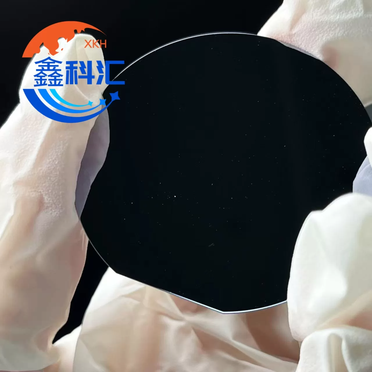
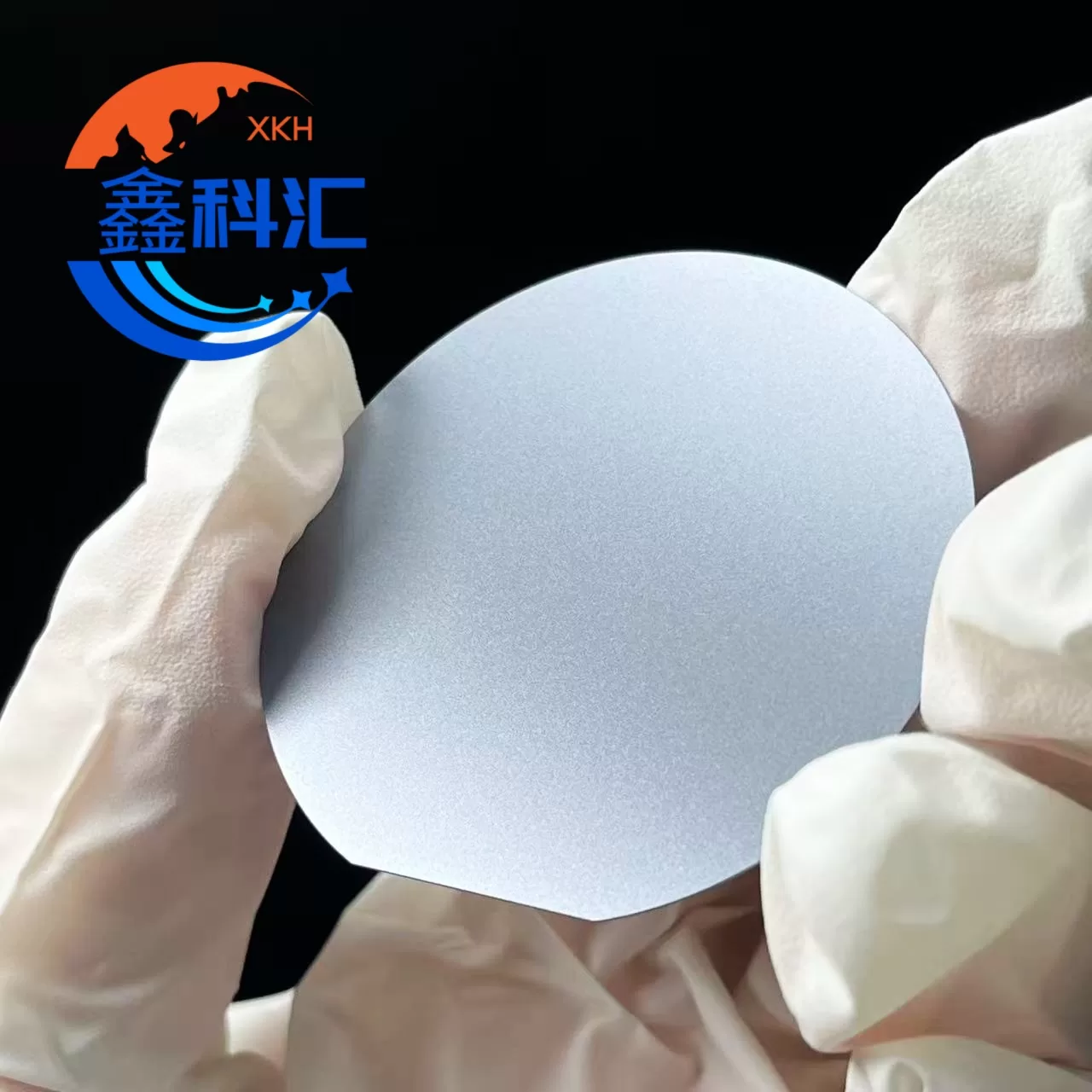
The 2-inch zinc-doped Gallium Arsenide (GaAs) wafer is a p-type compound semiconductor wafer manufactured through the Vertical Gradient Freeze (VGF) crystal growth technique. This growth method enables precise control over crystal composition and dopant distribution, resulting in uniform electrical properties and stable wafer-to-wafer performance.
Zinc is introduced as an acceptor dopant to achieve p-type conductivity with controlled carrier concentration and low resistivity. Combined with the inherent advantages of GaAs as a direct bandgap III–V semiconductor, this wafer delivers high optical emission efficiency, fast carrier response, and reliable electrical behavior. These characteristics make it well suited for light-emitting devices, laser diodes, and other optoelectronic components that require consistent wafer quality.
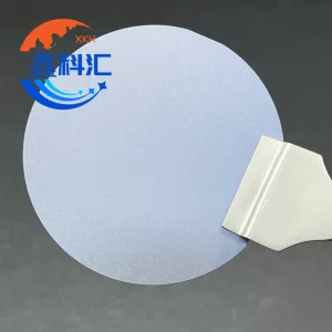
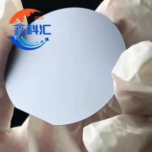

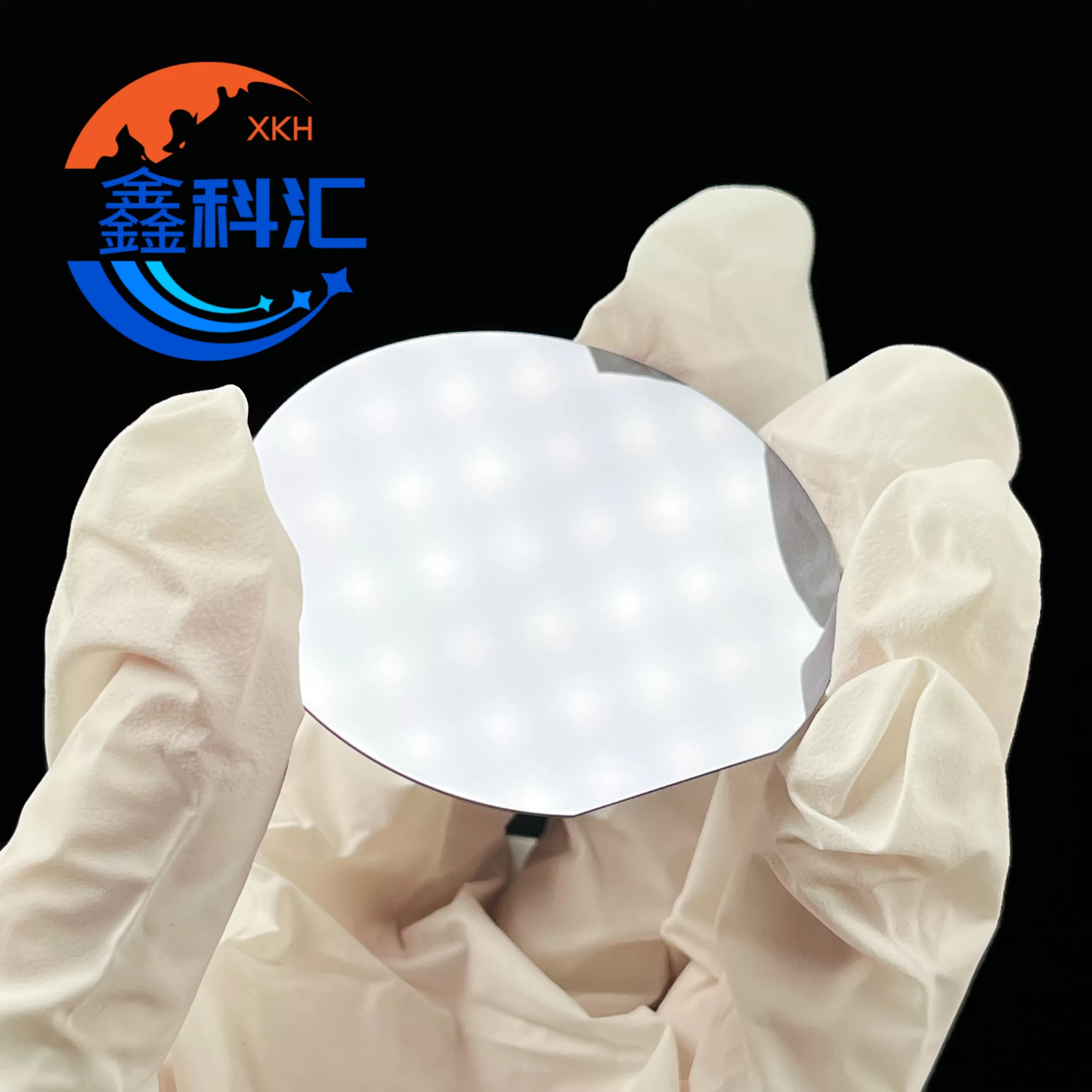
The wafer is produced with a standard (100) crystal orientation and optional misorientation angles to support optimized epitaxial layer growth. Polished surface finishes, low etch pit density, and strict flatness control allow the wafer to meet the requirements of advanced wafer processing, photolithography, and epitaxial deposition processes such as MBE and MOCVD.
Dimensional accuracy, surface cleanliness, and mechanical stability are tightly controlled throughout the manufacturing process. Optional orientation flats, notch configurations, and backside laser marking provide flexibility for equipment compatibility, automation, and traceability in production environments. The 2-inch Zn-doped GaAs wafer is suitable for both research-scale development and volume manufacturing workflows.
Material and Physical Characteristics
Gallium Arsenide is a crystalline III–V compound semiconductor with a zinc blende crystal structure. It exhibits a direct bandgap, high electron mobility, and excellent thermal and electrical stability under operating conditions commonly encountered in optoelectronic and high-frequency electronic devices. Zinc-doped GaAs wafers offer predictable p-type behavior, enabling repeatable device characteristics and improved yield.
Key physical properties include a density of approximately 5.32 g/cm³, a molecular weight of 144.64, and a melting point of approximately 1400 °C. The gray crystalline appearance and cubic lattice structure are typical of high-purity single-crystal GaAs material grown under controlled conditions.


Manufacturing and Quality Control
The wafer is grown using the Vertical Gradient Freeze method, which allows slow and controlled solidification of the GaAs crystal. This process minimizes thermal stress, reduces crystal defects, and improves dopant uniformity across the wafer surface.
Post-growth processing includes precision slicing, lapping, polishing, and cleaning to achieve the required thickness, surface roughness, and flatness specifications. Each wafer undergoes inspection for dimensional accuracy, surface quality, and electrical properties. Key parameters such as etch pit density, particle count, total thickness variation, bow, and warp are monitored to ensure consistency and reliability for downstream processing.
ข้อมูลจำเพาะทางเทคนิค
| Attribute | มูลค่า |
|---|---|
| วัสดุ | Gallium Arsenide (GaAs) |
| โดปานต์ | Zinc (Zn) |
| ชนิดเวเฟอร์ | P-Type Semiconductor Wafer |
| Crystal Growth Method | Vertical Gradient Freeze (VGF) |
| โครงสร้างผลึก | Zinc Blende |
| การเรียงตัวของผลึก | (100) ± 0.5° |
| Misorientation Options | 2° / 6° / 15° off (110) |
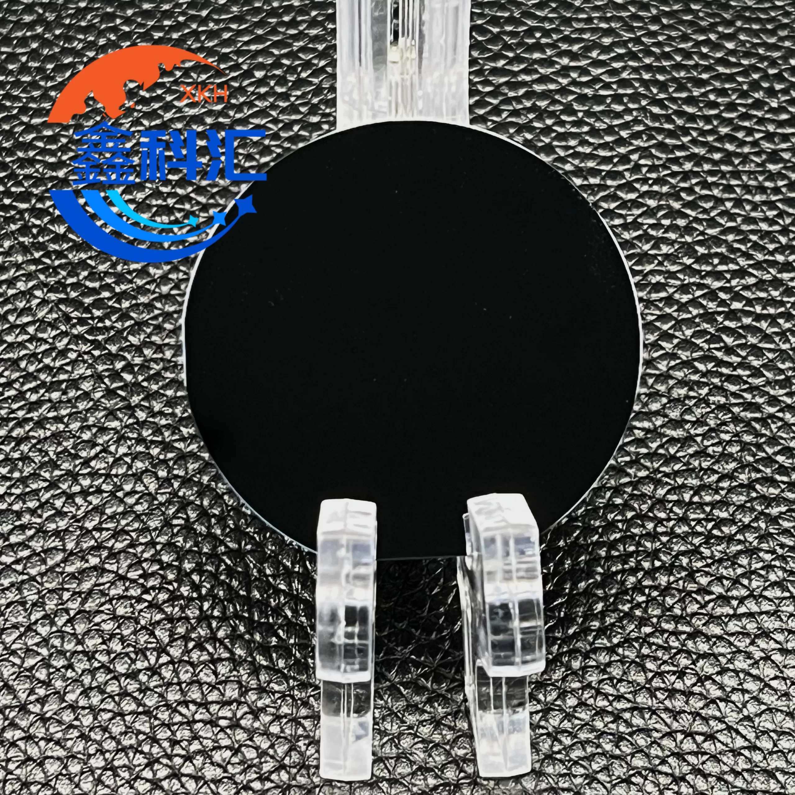
| เส้นผ่านศูนย์กลาง | 50.8 ± 0.2 mm |
| ความหนา | 220 – 350 ± 20 µm |
| Orientation Flat | 16 ± 1 mm |
| Identification Flat | 8 ± 1 mm |
| Flat / Notch Options | EJ, US, or Notch |
| ผิวสำเร็จ | P/P or P/E |
| ความเข้มข้นของตัวพาหะ | (0.3 – 1.0) × 10¹⁸ cm⁻³ |
| Electrical Resistivity | (0.8 – 9.0) × 10⁻³ Ω·cm |
| Hall Mobility | 1,500 – 3,000 cm²/V·s |
| Etch Pit Density | ≤ 5,000 cm⁻² |
| Total Thickness Variation | ≤ 10 µm |
| Bow / Warp | ≤ 30 µm |
| Particle Count | < 50 particles (≥ 0.3 µm per wafer) |
| Laser Marking | Backside or upon request |
| บรรจุภัณฑ์ | Single wafer container or cassette, aluminum composite outer bag |
| CAS Number | 1303-00-0 |
Application Areas
LED wafer processing and device fabrication
Laser diode wafer manufacturing
Optoelectronic and photonic devices
RF and high-frequency electronic components
Research and process development wafers
Frequently Asked Questions
Why is zinc doping used for GaAs wafers?
Zinc acts as an effective acceptor dopant in GaAs, providing stable p-type conductivity with controlled carrier concentration. This is critical for optoelectronic devices that rely on consistent hole transport and optical emission performance.
What makes this wafer suitable for epitaxial growth?
The combination of controlled crystal orientation, low defect density, polished surface finish, and strict flatness specifications allows the wafer to be directly used for MBE and MOCVD epitaxial growth processes.
Can this wafer be supplied with customized mechanical or identification features?
Yes. Orientation flats, notch options, backside laser marking, and selected surface or electrical parameters can be customized to meet specific equipment, automation, or process requirements.
รีวิว
ยังไม่มีบทวิจารณ์