
From Compute Density to Power Density
The scaling of AI systems is no longer limited by transistor counts or model architectures, but by the ability to deliver and dissipate power at unprecedented densities. Modern AI training clusters operate with tens of thousands of accelerators, each drawing hundreds to over a thousand watts. At this scale, power delivery efficiency and thermal stability become system-defining constraints.
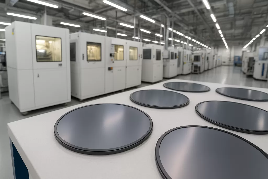
Twelve-inch silicon carbide wafers enter this landscape not as an incremental materials upgrade, but as an infrastructural pivot. They address a bottleneck that traditional silicon technologies cannot resolve: how to convert, distribute, and manage megawatts of power inside tightly packed AI clusters without sacrificing reliability or scalability.
Why AI Clusters Stress Power Electronics More Than Compute Logic
Unlike general-purpose data centers, AI clusters exhibit extreme load transients. Training workloads generate rapid, synchronized current spikes as thousands of GPUs or AI accelerators shift states simultaneously. These transients propagate through power distribution networks, causing voltage droop, electromagnetic interference, and thermal hotspots.
Conventional silicon-based power devices struggle in this regime. Their switching losses, thermal limits, and voltage handling capabilities impose architectural penalties: larger power modules, lower switching frequencies, and increased cooling overhead. As cluster sizes grow, these inefficiencies compound non-linearly.
This is where wide-bandgap materials, and specifically silicon carbide, become system-enabling rather than merely performance-enhancing.
The Material Advantage of SiC at the Cluster Scale
Silicon carbide combines a wide bandgap, high critical electric field, and superior thermal conductivity. These properties allow SiC power devices to operate at higher voltages, higher temperatures, and higher switching frequencies than their silicon counterparts.
At the cluster level, this translates into tangible architectural benefits. Higher switching frequencies shrink passive components, enabling compact power conversion modules that can be placed closer to the load. Higher voltage operation reduces current, lowering resistive losses across power distribution networks. Elevated temperature tolerance relaxes cooling constraints, improving overall energy efficiency.
While these advantages are well understood at the device level, their true impact emerges only when deployed across thousands of nodes in an AI cluster.
Why Wafer Diameter Matters for AI Infrastructure
The transition from 6-inch and 8-inch SiC wafers to 12-inch platforms is not driven solely by cost per die, although economies of scale are significant. The deeper implication lies in manufacturing uniformity and integration density.
Large-diameter wafers enable tighter statistical control over thickness, doping uniformity, and defect distributions. For power devices, this consistency directly affects breakdown voltage margins, on-resistance variability, and long-term reliability. In massive AI clusters, where millions of power devices operate continuously, even small parameter spreads translate into measurable system-level inefficiencies and failure risks.
Twelve-inch wafers also align SiC manufacturing with advanced CMOS production ecosystems. This compatibility accelerates heterogeneous integration, allowing SiC power devices to co-evolve with silicon logic and advanced packaging technologies rather than remaining a niche add-on.
Enabling High-Voltage Power Distribution Inside Data Centers
One of the most significant architectural shifts enabled by 12 inç SiC gofretler is the move toward higher-voltage, rack-level and board-level power distribution.
SiC devices fabricated on large wafers support consistent, high-yield production of high-voltage MOSFETs and diodes. These devices make it feasible to distribute power at hundreds or even thousands of volts within data centers, converting down to load voltages only at the point of use.
For AI clusters, this approach dramatically reduces copper losses, cable bulk, and thermal load. The result is not just improved efficiency, but greater freedom in physical layout, enabling denser compute packing without proportional increases in cooling infrastructure.
Thermal Density and the Hidden Role of SiC Substrates
Thermal management is often discussed in terms of heat sinks and liquid cooling, but the substrate itself plays a foundational role.
SiC’s high thermal conductivity allows power devices to act as efficient heat conduits rather than thermal bottlenecks. When fabricated on 12-inch wafers with uniform material quality, thermal impedance becomes predictable and designable at scale.
This predictability is critical in AI clusters, where thermal runaway in a single power module can cascade into localized failures. SiC’s thermal behavior supports more aggressive power densities while maintaining stable operating margins across thousands of identical units.
Reliability as a Scaling Constraint
In small systems, occasional component failure is manageable. In AI clusters with tens of thousands of nodes, reliability becomes a statistical problem.
The shift to 12-inch SiC wafers improves not only yield, but lifetime consistency. Lower defect densities, reduced micropipe occurrence, and tighter process control directly translate into longer mean time to failure. Over the operational lifespan of an AI data center, this reliability advantage compounds into lower maintenance costs and higher effective uptime.
From this perspective, 12-inch SiC wafers are not merely a manufacturing milestone, but a prerequisite for economically viable, ultra-scale AI infrastructure.
Beyond Power Devices: Toward System-Level Co-Design
The ultimate impact of 12-inch SiC wafers lies in their ability to integrate into a broader system-level design philosophy. As AI hardware moves toward co-packaged optics, advanced interposers, and three-dimensional integration, power delivery must evolve in parallel.
Large-diameter SiC wafers enable standardized, high-volume production of power components that can be architected as first-class citizens within AI systems, rather than external constraints. This convergence blurs the traditional boundary between power electronics and computing hardware.
Conclusion: SiC as an Enabler of AI at Scale
Massive AI chip clusters are often framed as a triumph of algorithms and compute architectures. Yet beneath this narrative lies a materials story.
Twelve-inch SiC wafers enable a new generation of power electronics that align with the scale, density, and reliability demands of modern AI systems. They do not make AI models smarter, but they make large-scale intelligence physically and economically feasible.
In the long arc of AI infrastructure, the transition to large-diameter SiC substrates may be remembered not as a manufacturing upgrade, but as a foundational shift that allowed computation to scale beyond the limits of silicon alone.