
Silicon Carbide (SiC) has gained increasing attention as a wide-bandgap semiconductor material for power devices over the past two decades. Compared to silicon (Si), SiC devices offer significant advantages such as higher breakdown electric fields, faster switching speeds, better thermal conductivity, and higher operating temperatures. However, the realization of these advantages requires advanced packaging technologies to address challenges such as reducing parasitic inductance, enhancing thermal performance, and ensuring reliability at high temperatures. This paper provides an overview of the latest developments in SiC power device packaging technologies, focusing on low parasitic inductance, high-temperature packaging, and multifunctional integrated packaging. The challenges and opportunities in these areas are also discussed.
Introduction:
Silicon Carbide (SiC) power devices are poised to revolutionize power electronics due to their superior material properties compared to traditional silicon devices. SiC-based power devices can operate at higher frequencies, voltages, and temperatures, resulting in improved efficiency and power density for various applications, including electric vehicles, renewable energy systems, and industrial power electronics. However, these advantages can only be fully realized through the development of advanced packaging technologies that address the unique requirements of SiC devices.
1. Low Parasitic Inductance Packaging Technology:
The reduction of parasitic inductance in SiC power device packaging is critical for achieving high-speed switching and minimizing voltage overshoot and electromagnetic interference (EMI). Traditional packaging structures, commonly used for silicon devices, suffer from high parasitic inductance due to large switching loops and the use of metal bond wires. To address this issue, several innovative packaging technologies have been developed.
1.1 Flip-Chip Packaging:
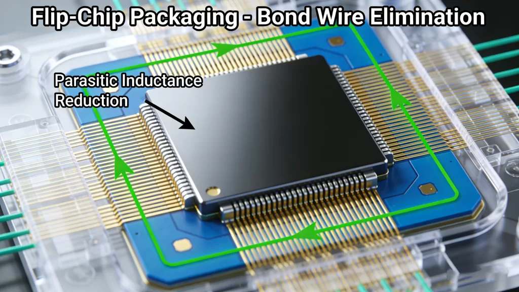
Flip-chip packaging technology, such as the one proposed by the University of Arkansas team, uses a metal interconnect to flip the chip and connect the backside electrode to the same plane as the front electrode. This eliminates the need for bond wires and significantly reduces parasitic inductance. This packaging approach has been shown to reduce the device size by 14 times and the on-state resistance by 24% compared to traditional TO-247 packaging.
1.2 DBC+PCB Hybrid Packaging:
Another solution to reduce parasitic inductance involves combining Direct Bonded Copper (DBC) and Printed Circuit Boards (PCB) in a hybrid packaging structure. By connecting the chip’s surface to the PCB, the current loop area is minimized, leading to a significant reduction in parasitic inductance. This hybrid packaging can achieve inductance values below 5nH and reduce the overall volume by 40%.
1.3 Chip-on-Lead Interconnection:
The use of direct lead bonding (DLB) for chip-to-lead connections further minimizes the current loop area, thereby reducing parasitic inductance and improving temperature cycling performance and reliability. This packaging technique eliminates the need for bond wires, making it a promising solution for SiC power devices.
1.4 Dual-Sided Cooling Packaging:
Dual-sided cooling technology, commonly used in power electronics for electric vehicles, has been applied to SiC devices to improve heat dissipation. By using DBC substrates on both sides of the chip, the package achieves simultaneous heat dissipation from both the top and bottom surfaces. This reduces the thermal resistance by 38% compared to traditional packaging.
1.5 3D Packaging Technology:
3D packaging technology takes advantage of SiC’s vertical structure to reduce parasitic inductance. By stacking switching arms directly on top of each other, 3D packaging eliminates unnecessary wiring and significantly reduces loop inductance to below 1nH. This approach has been shown to improve both the efficiency and power density of the device.
2. High-Temperature Packaging Technology:
SiC power devices are designed to operate at temperatures exceeding 300°C, far higher than traditional silicon devices. However, the packaging materials and structures used in silicon devices are not suitable for high-temperature applications, as their reliability decreases significantly above 150°C. Therefore, the development of packaging materials that can withstand high temperatures is crucial for the success of SiC power devices.
2.1 High-Temperature Interconnection Materials:
Copper bonding wires, which replace aluminum wires in high-temperature applications, significantly improve the reliability of SiC power devices. Additionally, copper tapes and bands are being explored for their superior current-carrying capacity and heat dissipation ability, making them ideal for high-temperature SiC applications.
2.2 Sintered Silver Technology:
Sintered silver bonding is emerging as an alternative to traditional soldering techniques for high-temperature applications. With a thermal conductivity of 200W/(m·K), sintered silver provides excellent thermal management and high melting points, making it ideal for SiC power devices. However, the process to optimize sintered silver bonding—particularly regarding pressure, temperature, and time—remains an area of active research.
2.3 Ceramic Substrates and Metal Base Plates:
To ensure the long-term reliability of SiC power devices in high-temperature environments, the substrates and base plates must exhibit high thermal conductivity and match the coefficient of thermal expansion (CTE) of SiC. Materials such as Aluminum Nitride (AlN) and Beryllium Oxide (BeO) are being considered due to their excellent thermal properties. However, BeO’s toxicity limits its widespread use, and AlN’s high cost remains a barrier to its adoption.
3. Multifunctional Integrated Packaging Technology:
As SiC devices are pushed towards miniaturization and higher power densities, multifunctional integration is becoming increasingly important. The integration of capacitors, drivers, sensors, and heat sinks into the packaging is crucial to improving the overall performance of the device.
3.1 Integrated Capacitors and Drivers:
The integration of ceramic capacitors directly within the power module reduces parasitic inductance and improves overall system performance. However, the high-temperature reliability of these capacitors is still a challenge. Similarly, integrating gate drivers within the module, as seen in SiC intelligent power modules (IPMs) from companies like Mitsubishi and Infineon, reduces the size of the module and improves switching performance.
3.2 Sensor Integration and EMI Mitigation:
Temperature, current, and voltage sensors are being integrated into SiC power devices to provide real-time monitoring and control, enhancing the overall performance and reliability of the system. Additionally, EMI filters and shielding are integrated to mitigate electromagnetic interference, ensuring compliance with industry standards.
3.3 Microchannel Heat Sink Integration:
Microchannel heat sinks are being integrated directly into the power module to improve heat dissipation. This technology reduces the thermal resistance and improves the overall thermal performance of SiC power devices. The integration of microchannel cooling within the module’s baseplate can result in a 34% reduction in thermal resistance.
4. Challenges and Future Prospects:
Despite the advancements in SiC packaging technologies, several challenges remain, particularly in the areas of material development, cost reduction, and high-temperature reliability. Further research is needed to:
- Validate the performance of low parasitic inductance packaging structures, especially in terms of power cycling, thermal cycling, and overall reliability.
- Develop high-temperature packaging materials with optimal thermal conductivity and thermal expansion properties.
- Overcome the limitations of ceramic capacitors, sensors, and other integrated components at high temperatures.
- Explore new cooling technologies, such as microchannel cooling and phase change materials, to further enhance the thermal performance of SiC power devices.
In conclusion, the development of advanced packaging technologies is key to unlocking the full potential of SiC power devices. As the industry continues to innovate, SiC will play an increasingly important role in the evolution of power electronics, paving the way for higher efficiency, higher power density, and more reliable systems.