
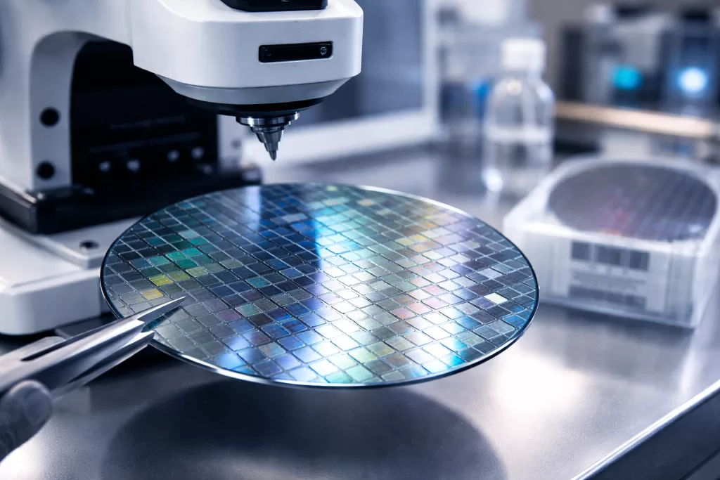
In the field of Microelectromechanical Systems (MEMS), device performance is highly sensitive to material quality at the micro- and nanoscale. Among all substrate parameters, surface roughness of custom prime grade silicon wafers plays a critical yet often underestimated role. While electrical properties and crystallographic orientation are commonly prioritized, surface topology directly influences mechanical reliability, thin-film integrity, and overall device yield.
1. What Is Surface Roughness in Silicon Wafers?
Surface roughness refers to the microscopic variations in height across a wafer surface. It is typically quantified using parameters such as:
- Ra (Average Roughness) – arithmetic mean deviation
- Rq (Root Mean Square Roughness) – more sensitive to peaks/valleys
- Rz (Peak-to-Valley Height) – extreme surface variation
For prime grade silicon wafers, roughness is usually controlled at the angstrom to sub-nanometer level, especially for advanced MEMS fabrication.
Typical Roughness Ranges
| Wafer Type | Surface Roughness (Ra) |
|---|---|
| Prime Grade (Polished) | 0.1 – 0.5 nm |
| Epitaxial Wafer | < 0.3 nm |
| Test Grade | 1 – 10 nm |
2. Why Surface Roughness Matters in MEMS
2.1 Impact on Thin Film Deposition
MEMS devices rely heavily on thin films such as:
- Silicon dioxide (SiO₂)
- Silicon nitride (Si₃N₄)
- Metal layers (Al, Au, Pt)
A rough substrate surface can cause:
- Non-uniform film thickness
- Poor adhesion
- Increased defect density
This directly affects device reliability and performance.
2.2 Mechanical Performance and Stress Concentration
MEMS structures such as cantilevers, beams, and diaphragms are extremely sensitive to surface imperfections.
Higher roughness leads to:
- Stress concentration points
- Reduced fracture strength
- Lower fatigue life
In high-frequency MEMS resonators, even nanometer-scale roughness can introduce energy dissipation, lowering the Q-factor.
2.3 Etching Uniformity and Process Control
Surface roughness affects both wet and dry etching processes:
- Non-uniform etch rates
- Micro-masking effects in plasma etching
- Increased surface scattering
For processes like DRIE (Deep Reactive Ion Etching), smooth surfaces ensure:
- Vertical sidewalls
- Consistent feature dimensions
2.4 Wafer Bonding Quality
MEMS fabrication often involves wafer bonding techniques such as:
- Direct (fusion) bonding
- Anodic bonding
Surface roughness directly impacts bonding strength:
| Roughness Level | Bonding Outcome |
|---|---|
| < 0.5 nm | Strong atomic bonding |
| 0.5–1 nm | Partial bonding |
| > 1 nm | Void formation |
Even slight roughness increases can lead to:
- Voids at the interface
- Reduced hermetic sealing
- Device failure in packaging
2.5 Optical and Sensor Performance
In optical MEMS (MOEMS), surface roughness affects:
- Light scattering
- Reflectivity
- Signal-to-noise ratio
For sensors such as pressure or inertial devices, roughness can introduce:
- Measurement drift
- Reduced sensitivity
3. Measurement Techniques for Surface Roughness
Accurate measurement is essential for quality control.
Common Methods
| Method | Resolution | Application |
|---|---|---|
| AFM (Atomic Force Microscopy) | < 0.1 nm | Ultra-smooth surfaces |
| Optical Profilometry | ~1 nm | Fast inspection |
| Stylus Profilometer | ~1 nm | General-purpose |
| SEM (Scanning Electron Microscopy) | Visual | Structural analysis |
Among these, AFM is the industry standard for MEMS-grade wafers.
4. Customization Requirements for MEMS Wafers
Custom prime wafers are often specified with tight surface constraints depending on application.
Key Parameters to Define
- Surface roughness (Ra, Rq)
- Wafer diameter (e.g., 4″, 6″, 8″, 12″)
- Orientation (100), (111)
- Doping type and resistivity
- Double-side polishing (DSP) vs single-side
Example Specification Table
| Parameter | Typical MEMS Requirement |
|---|---|
| Surface Roughness | ≤ 0.3 nm (Ra) |
| Flatness (TTV) | ≤ 1 µm |
| Warp/Bow | < 30 µm |
| Cleanliness | Class 1 or better |
5. Trade-offs: Cost vs Performance
Lower roughness means:
- More advanced polishing (CMP)
- Higher production cost
However, insufficient surface quality can lead to:
- Yield loss
- Device failure
- Increased downstream processing cost
Engineering insight:
It is often more cost-effective to invest in higher-grade wafers than to compensate for defects later in fabrication.
6. Practical Selection Guidelines
When selecting custom prime silicon wafers for MEMS:
Choose ultra-low roughness when:
- Wafer bonding is required
- High-Q resonators are used
- Optical MEMS applications are involved
Moderate roughness may be acceptable when:
- Bulk micromachining dominates
- Surface films are thick (>1 µm)
- Cost constraints are critical
7. Conclusion
Surface roughness is not just a secondary specification—it is a core determinant of MEMS device performance and reliability. From thin-film deposition to wafer bonding and mechanical integrity, nanometer-scale variations can have system-level consequences.
For engineers and procurement teams, understanding and specifying the correct roughness level ensures:
- Higher yield
- Better device consistency
- Lower long-term cost
In the increasingly demanding MEMS landscape, surface precision is no longer optional—it is foundational.