
SiC Wafer Manufacturing Challenges: Crystal Growth, Slicing, and Polishing
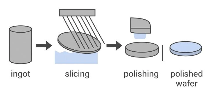
Silicon Carbide (SiC) has emerged as one of the most important semiconductor materials for next-generation power electronics. Thanks to its wide bandgap, high thermal conductivity, and superior breakdown electric field, SiC devices offer significant advantages over traditional silicon-based technologies in electric vehicles, renewable energy systems, industrial drives, and high-voltage power conversion. Despite these advantages, manufacturing […]
N-Type vs. Semi-Insulating SiC Wafers: Main Differences and Applications
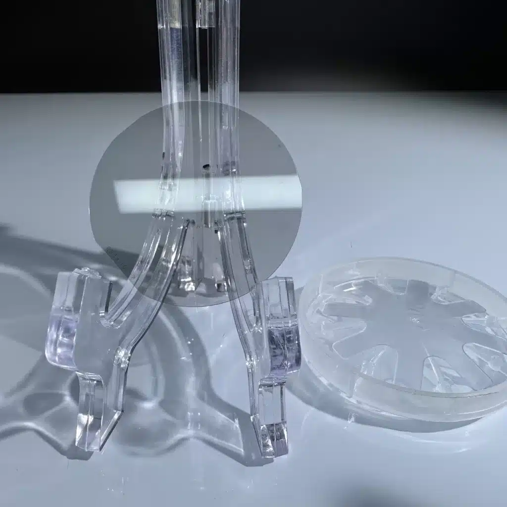
Silicon carbide (SiC) wafers have become one of the most important wide-bandgap semiconductor substrates in power electronics, RF communication, and high-temperature applications. Among the most widely used types are N-type SiC wafers and semi-insulating SiC wafers. Although they may look similar physically, their electrical behavior and application fields are fundamentally different. Choosing the wrong type […]
Ceramics vs Sapphire vs Silicon Carbide in Semiconductor Manufacturing
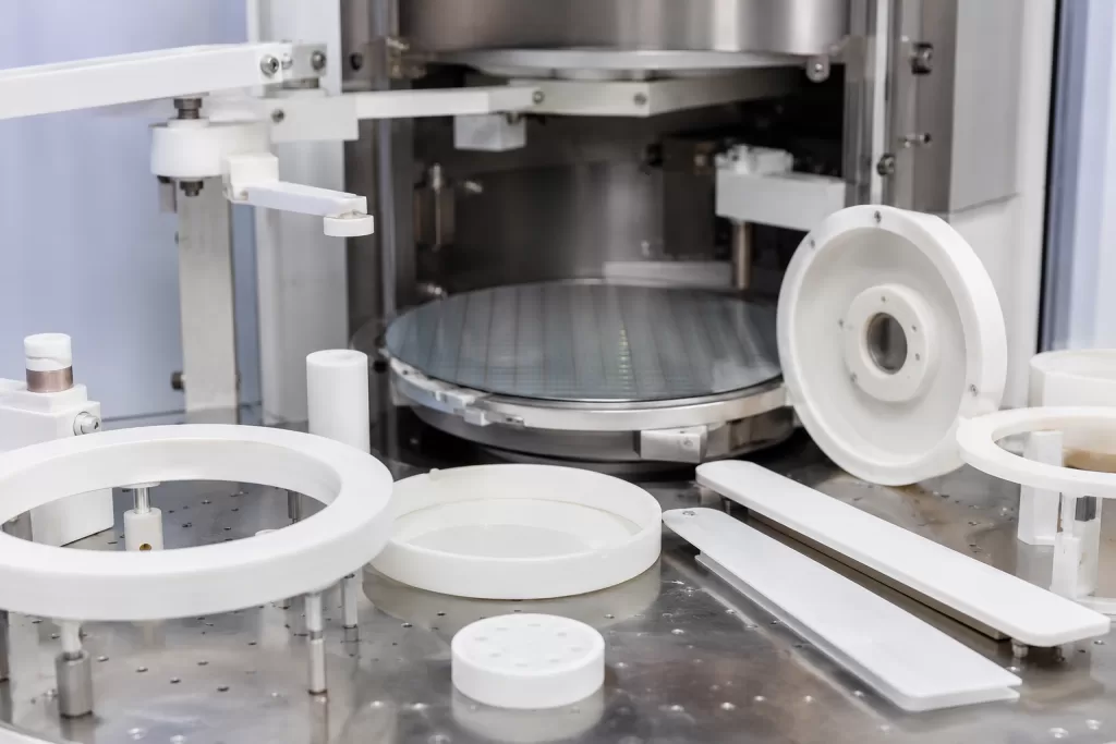
As semiconductor technology advances toward smaller process nodes, larger wafer sizes, and increasingly complex manufacturing environments, material selection has become a critical engineering consideration. Modern semiconductor equipment operates under extreme conditions involving ultra-high temperatures, plasma exposure, corrosive process gases, vacuum environments, and strict contamination requirements. Under such conditions, conventional engineering materials often struggle to meet […]
Semiconductor Materials in 2026: Fundamentals, Classification, and Emerging Directions

Semiconductor materials form the physical foundation of modern electronics, enabling technologies ranging from integrated circuits and power devices to photonics and quantum systems. Defined by electrical conductivity intermediate between metals and insulators, semiconductors derive their functionality from tunable electronic structures. By 2026, the field has evolved beyond traditional silicon, driven by demands in artificial intelligence, […]
Silicon Carbide (SiC): The Enabling Material for AI Chip Packaging and Next-Generation Server Power Systems
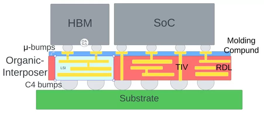
With the rapid expansion of artificial intelligence workloads, both data centers and advanced semiconductor devices are facing unprecedented challenges in power consumption and thermal management. Leading platforms from companies such as Intel and NVIDIA are pushing system power levels to new extremes. Server racks are moving from tens of kilowatts to over 100 kW, while […]
Why Silicon Carbide Substrates Have Become a “Must-Have Material” for New Energy and 5G
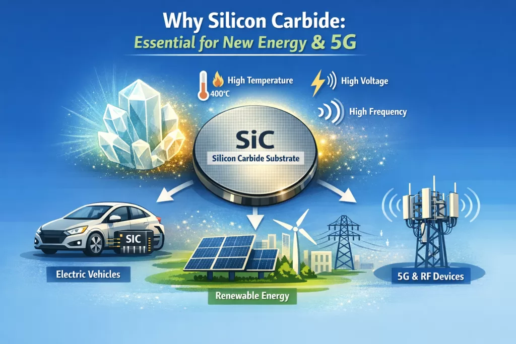
1. Introduction: From Silicon Limits to Wide Bandgap Breakthroughs As global industries accelerate toward electrification and digitalization, conventional silicon (Si)-based semiconductors are approaching their physical and performance limits. Applications such as electric vehicles, renewable energy systems, and 5G communications demand devices that can operate under higher voltages, higher temperatures, and higher frequencies. In this context, […]
Silicon Carbide Industry: Production Factors and Capacity Overview
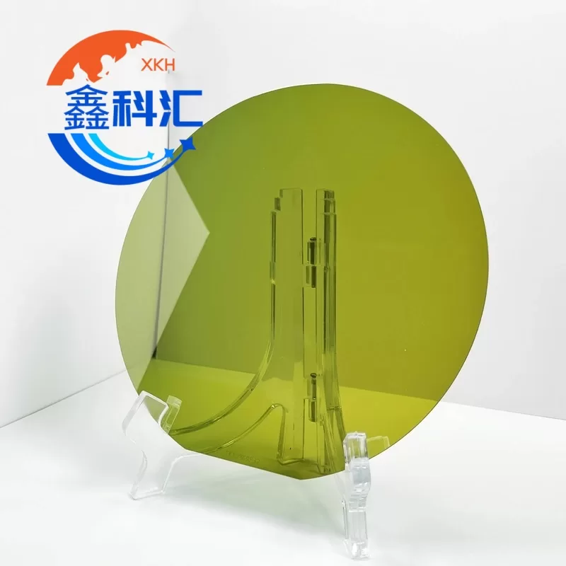
Silicon carbide (SiC) has emerged as one of the leading representatives of third-generation semiconductors, offering significant advantages over conventional silicon in terms of wider bandgap, higher breakdown electric field, and superior thermal conductivity. These properties make SiC highly suitable for high-temperature, high-voltage, and high-frequency applications. Its exceptional physical and chemical characteristics enable the production of […]
Custom Prime Grade Silicon Wafers: Why Surface Roughness Matters for MEMS
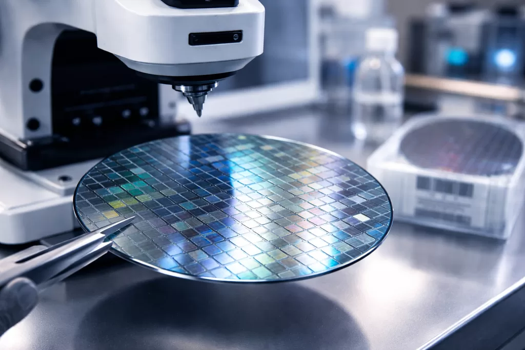
In the field of Microelectromechanical Systems (MEMS), device performance is highly sensitive to material quality at the micro- and nanoscale. Among all substrate parameters, surface roughness of custom prime grade silicon wafers plays a critical yet often underestimated role. While electrical properties and crystallographic orientation are commonly prioritized, surface topology directly influences mechanical reliability, thin-film […]