
Silicon is often described as a hard but brittle material. This description is correct, but it can also be misleading.
How hard is silicon actually?
Is silicon harder than steel? How does it compare with glass? And why is silicon carbide significantly more difficult to grind, polish and dice even though both silicon and SiC are widely used as semiconductor wafer materials?
The answer depends partly on how hardness is measured.
Mohs hardness, Vickers hardness and Knoop hardness measure different aspects of a material’s resistance to deformation or scratching. Their numerical values cannot be directly converted without considering the material, test load, crystal orientation and test method.
For semiconductor engineers, understanding these differences is useful when evaluating:
- Wafer slicing
- Grinding
- Lapping
- CMP polishing
- Wafer dicing
- Edge chipping
- Surface damage
- Abrasive selection
- Tool wear
This guide compares the hardness of silicon, silicon carbide, glass and steel and explains what the numbers mean in practical semiconductor processing.
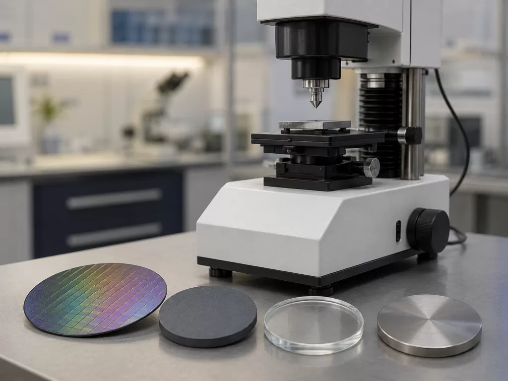
Quick Comparison: Silicon vs. SiC vs. Glass vs. Steel
The following table gives representative hardness ranges. Values should be considered approximate because measured hardness varies with material grade, crystal orientation, test load and measurement conditions.
| Material | Mohs Hardness | Representative Vickers Hardness | General Behavior |
|---|---|---|---|
| Silicon | ~7 | ~1,000–1,300 HV | Hard and brittle |
| Silicon Carbide | ~9–9.5 | ~2,500–2,800 HV or higher | Extremely hard and brittle |
| Fused Silica / Quartz Glass | ~5.5–6.5 | ~880–1,000 HV equivalent range | Hard, brittle glass |
| Typical Annealed Alloy Steel | ~4–5* | ~200–330 HV | Softer but much tougher |
*Mohs values for metals are only rough comparisons because Mohs testing was originally developed for minerals.
Heraeus lists fused quartz and fused silica at approximately 5.5–6.5 Mohs hardness, with Knoop hardness around 5.8–6.2 GPa.
Commercial SiC ceramics can reach approximately 2,500–2,800 kgf/mm² Vickers hardness, depending on composition and processing.
The important conclusion is:
SiC is considerably harder than silicon, while silicon is generally harder than common glass and many steels in terms of scratch or indentation resistance.
But hardness alone does not tell us which material is easier to break.
What Does “Hardness” Actually Mean?
Hardness generally describes a material’s resistance to localized deformation, penetration, scratching or abrasion.
However, different hardness tests measure this resistance differently.
Three tests are especially relevant when discussing semiconductor and optical materials:
- Mohs hardness
- Vickers hardness
- Knoop hardness
They should not be treated as interchangeable scales.
1. Mohs Hardness
The Mohs scale measures scratch resistance.
A harder reference material scratches a softer one.
The scale ranges from:
- 1 — Talc
- 2 — Gypsum
- 3 — Calcite
- 4 — Fluorite
- 5 — Apatite
- 6 — Orthoclase
- 7 — Quartz
- 8 — Topaz
- 9 — Corundum
- 10 — Diamond
Silicon is generally reported at approximately:
Mohs hardness ≈ 7
Silicon carbide is significantly harder:
Mohs hardness ≈ 9–9.5
This immediately explains why SiC requires more aggressive machining technology than silicon.
But there is an important limitation.
Mohs Is Not a Linear Scale
A material with Mohs hardness 9 is not simply “29% harder” than one with Mohs hardness 7.
The scale is ordinal rather than linear.
The difference in actual indentation or abrasion resistance between materials near the upper end of the Mohs scale can be very large.
Therefore, Mohs hardness is useful for quick comparisons but is less useful for precision engineering.
2. Vickers Hardness
Vickers testing provides a much more quantitative measurement.
A diamond indenter shaped as a square-based pyramid is pressed into the material under a controlled load.
The dimensions of the indentation are then measured.
The result is normally expressed as:
HV — Vickers Hardness
or historically:
kgf/mm²
Vickers testing is widely used for:
- Metals
- Ceramics
- Semiconductor materials
- Coatings
- Thin components
The Vickers method uses a diamond pyramid with a 136° angle between opposite faces.
Because the test produces a measurable indentation rather than simply checking whether one material scratches another, it provides more useful engineering data.
Silicon Vickers Hardness
Typical crystalline silicon values are approximately:
1,000–1,300 HV
This corresponds roughly to:
9.8–12.7 GPa
depending on crystal orientation, surface condition and indentation load.
This makes silicon much harder than many conventional structural metals.
However, silicon remains extremely brittle.
That distinction is very important.
A hardened steel component may resist fracture or impact much better than a silicon wafer despite having lower indentation hardness.
Silicon Carbide Vickers Hardness
SiC is much harder.
Representative commercial SiC materials often show Vickers hardness around:
2,500–2,800 HV
or roughly:
24–28 GPa
Some measurements may be higher depending on SiC polytype, crystal quality, crystal plane and indentation conditions. Commercial SiC values around 27.5 GPa have been reported in published materials research.
This means that from a machining perspective:
SiC is roughly about twice as resistant to indentation as silicon under many comparable conditions.
This is one reason why diamond tooling plays such an important role in SiC processing.
3. Knoop Hardness
Knoop hardness testing is similar to Vickers testing but uses a different diamond indenter.
Instead of producing a relatively symmetrical square indentation, the Knoop indenter creates an elongated, shallow indentation.
This characteristic makes Knoop testing particularly useful for:
- Brittle materials
- Glass
- Ceramics
- Semiconductor wafers
- Thin layers
- Coatings
- Small test areas
Because penetration depth is relatively shallow, Knoop testing can reduce the risk of severe cracking in fragile specimens.
This makes it particularly relevant to semiconductor wafer characterization.
Why Knoop Hardness Is Useful for Silicon and SiC
Semiconductor wafers are usually:
- Relatively thin
- Brittle
- Highly polished
- Crystal-orientation dependent
A deep indentation may generate cracks or interact with subsurface damage.
Knoop testing allows hardness to be measured using comparatively shallow penetration.
For silicon wafers, measured hardness can vary with crystal orientation.
Typical Knoop values may fall around:
1,000–1,300 HK
depending on crystal direction and test conditions.
For SiC, the values are much higher.
Research on 4H-SiC and 6H-SiC single crystals demonstrates another important characteristic: measured Knoop hardness changes considerably with indentation load.
For example, measurements on 4H-SiC reported average hardness values ranging from approximately 39.5 GPa at 0.49 N to about 19.5 GPa at 19.61 N.
This illustrates why a SiC hardness specification should ideally include:
Hardness value + test method + indentation load + crystal plane
rather than publishing only a single number.
Mohs vs. Vickers vs. Knoop: What’s the Difference?
| Test | Mohs | Vickers | Knoop |
| Main Measurement | Scratch resistance | Indentation resistance | Micro-indentation resistance |
| Indenter | Reference material | Diamond pyramid | Elongated diamond |
| Result | 1–10 | HV | HK |
| Quantitative | Limited | Yes | Yes |
| Suitable for Silicon | Basic comparison | Yes | Excellent |
| Suitable for SiC | Basic comparison | Yes | Excellent |
| Suitable for Thin Samples | Limited | Possible | Very suitable |
| Crystal Orientation Analysis | Limited | Possible | Very useful |
For semiconductor engineering, Vickers and Knoop hardness are usually much more meaningful than Mohs hardness.
Mohs values remain useful primarily for simple material comparisons and general educational purposes.
Is Silicon Harder Than Glass?
In most common comparisons:
Yes.
Crystalline silicon has a Mohs hardness around 7.
Heraeus reports fused quartz and fused silica at approximately:
5.5–6.5 Mohs
with Knoop hardness approximately:
5.8–6.2 GPa.
Silicon therefore generally offers greater scratch and indentation resistance than common glass materials.
However, the term glass covers a very broad range of compositions.
Examples include:
- Soda-lime glass
- Borosilicate glass
- Fused silica
- Aluminosilicate glass
- Chemically strengthened glass
- Optical glass
Their hardness can differ significantly.
Therefore, engineers should specify the glass composition before making a precise comparison.
Is Silicon Harder Than Steel?
This question produces one of the most interesting comparisons.
In terms of scratch or indentation hardness:
Silicon can be harder than many common steels.
For example, some annealed alloy steels have Vickers hardness around:
200–330 HV
depending on alloy and heat treatment.
Published data for AISI 8625H alloy steel gives approximately 211 HV, while another higher-strength alloy example reaches approximately 329 HV.
Compare that with silicon at roughly:
1,000–1,300 HV.
Silicon can therefore show several times the indentation hardness of conventional annealed steel.
But if you drop a silicon wafer and a steel plate onto the floor, the silicon wafer is much more likely to break.
Why?
Because:
Hardness is not the same as toughness.
Hardness vs. Toughness
This distinction is extremely important in semiconductor processing.
Hardness
Hardness measures resistance to:
- Scratching
- Indentation
- Local plastic deformation
- Abrasive wear
Toughness
Toughness describes a material’s ability to absorb energy before fracturing.
A material can therefore be:
very hard but very brittle
or:
relatively soft but very tough.
Silicon and SiC belong primarily to the first category.
Steel belongs primarily to the second.
Why Silicon Wafers Can Break Even Though Silicon Is Hard
A silicon wafer resists surface indentation relatively well.
But silicon is a crystalline brittle material.
Defects such as:
- Edge chips
- Microcracks
- Scratches
- Grinding damage
- Dicing damage
- Subsurface cracks
can become stress concentration points.
Once a crack begins propagating, the wafer may fracture rapidly.
This is why semiconductor wafer processing must control both:
surface hardness-related machining
and
fracture-related mechanical damage.
Why SiC Is More Difficult to Machine Than Silicon
The hardness difference between silicon and silicon carbide has major manufacturing consequences.
SiC combines:
- Very high hardness
- High elastic modulus
- Strong chemical stability
- High thermal stability
- Brittle fracture behavior
This creates challenges during nearly every mechanical processing step.
SiC Crystal Slicing
SiC boule slicing generally requires highly wear-resistant abrasive systems.
Diamond abrasives are commonly used because conventional abrasive materials may experience rapid wear when processing SiC.
The high hardness of SiC affects:
- Cutting speed
- Wire wear
- Kerf loss
- Surface damage
- Cutting forces
SiC Grinding
Wafer grinding removes material to control:
- Thickness
- TTV
- Bow
- Warp
- Surface condition
Because SiC is extremely hard, grinding wheel selection and process control become especially important.
Incorrect grinding parameters may create:
- Microcracks
- Subsurface damage
- Edge chipping
- Excessive wheel wear
SiC Polishing
Mechanical polishing alone is inefficient for producing an epi-ready SiC surface.
Therefore, chemical mechanical polishing (CMP) combines chemical surface modification with controlled mechanical removal.
The purpose is not simply to “scratch away” the SiC surface.
Instead, the process makes the surface easier to remove while minimizing crystal damage.
SiC Wafer Dicing
Hardness also affects wafer dicing.
Compared with silicon, SiC generally causes:
- Greater blade wear
- Lower achievable feed rates
- Increased chipping risk
- Higher process forces
- Greater sensitivity to blade selection
The dicing system must therefore balance:
material removal rate + blade life + kerf quality + chipping control.
Does Higher Hardness Mean Better Wear Resistance?
Usually, increased hardness improves resistance to abrasive wear.
However, hardness alone cannot predict component lifetime.
Wear also depends on:
- Fracture toughness
- Surface roughness
- Counterface material
- Particle size
- Load
- Sliding speed
- Temperature
- Chemical environment
CoorsTek similarly notes that hardness alone does not completely determine abrasive wear behavior; material removal can also depend on surface ductility, particle shape, particle size and toughness.
Therefore, selecting semiconductor equipment materials solely according to the highest hardness value can be misleading.
Why Crystal Orientation Matters
Single-crystal materials are anisotropic.
This means some mechanical properties change depending on crystallographic direction.
For silicon, commonly used wafer orientations include:
- Si (100)
- Si (110)
- Si (111)
For SiC:
- 4H-SiC (0001)
- Off-axis 4H-SiC
- Different crystallographic directions within the basal plane
Indentation response, crack propagation and polishing behavior may vary with orientation.
Research on 4H-SiC and 6H-SiC demonstrates measurable changes in Knoop hardness with crystal direction as well as indentation load.
For precision research, therefore, simply specifying:
“SiC hardness = X”
is incomplete.
A better specification may be:
4H-SiC (0001), Knoop hardness, specified load and measurement direction.
Why Test Load Matters
Microhardness measurements can show an indentation size effect.
Measured hardness may change as indentation load changes.
This is particularly noticeable in very hard brittle materials such as SiC.
For example, published SiC measurements show hardness decreasing substantially as the indentation load increases.
Possible factors include:
- Elastic recovery
- Crack formation
- Surface condition
- Indentation geometry
- Crystal anisotropy
- Subsurface defects
Therefore, two suppliers may report different SiC hardness values without either measurement necessarily being incorrect.
The testing conditions must be compared.
Can Mohs Hardness Be Converted Directly to Vickers Hardness?
Not accurately.
Mohs hardness is based on scratch ranking.
Vickers hardness is based on resistance to controlled diamond indentation.
Therefore:
Mohs 7 ≠ a fixed Vickers value
and
Mohs 9 ≠ a fixed multiple of Mohs 7.
Conversion charts can provide approximate relationships, but they should not be used as precision engineering data.
For wafer or ceramic specifications, always use the actual measurement method required by the application.
Practical Hardness Ranking
For a simplified engineering comparison:
Typical Steel < Glass < Silicon << Silicon Carbide < Diamond
This ranking helps explain several familiar processing observations.
Steel
Relatively easy to machine with conventional cutting tools and capable of significant plastic deformation.
Glass
Harder and brittle, requiring abrasive grinding or specialized cutting.
Silicon
Harder than ordinary glass and many steels but highly brittle, requiring controlled wafer processing.
Silicon Carbide
Extremely hard, requiring diamond-based and advanced chemical-mechanical processing.
Diamond
The benchmark abrasive for machining many high-hardness semiconductor and ceramic materials.
What Hardness Means When Selecting a Wafer Material
Hardness should never be evaluated alone.
When comparing silicon and SiC wafers, engineers should also consider:
- Young’s modulus
- Fracture toughness
- Thermal conductivity
- Thermal expansion
- Chemical resistance
- Crystal orientation
- Surface roughness
- Subsurface damage
- Wafer thickness
- Bow and warp
For example, SiC’s very high hardness is beneficial for:
- Wear resistance
- Mechanical stability
- Harsh environments
but creates manufacturing challenges involving:
- Cutting
- Grinding
- Polishing
- Dicing
- Tool wear
Every advantageous material property creates its own processing trade-offs.
FAQ
What is the Mohs hardness of silicon?
Crystalline silicon is commonly reported at approximately 7 on the Mohs scale.
This makes it harder than many glasses and conventional metals but significantly softer than silicon carbide or diamond.
What is the Vickers hardness of silicon?
Typical values are around 1,000–1,300 HV, although results vary with crystallographic orientation, indentation load and testing conditions.
What is the hardness of silicon carbide?
SiC is approximately 9–9.5 on the Mohs scale.
Representative commercial SiC materials can reach approximately 2,500–2,800 HV, while measured single-crystal values vary according to polytype, crystal plane and test load.
Is silicon harder than steel?
In terms of indentation and scratch resistance, silicon is harder than many common steels.
However, steel is generally much tougher and more resistant to impact fracture.
Is silicon harder than glass?
Generally yes.
Silicon is approximately Mohs 7, while fused silica is typically around Mohs 5.5–6.5. Exact values depend on the type of glass.
Which is harder, silicon or silicon carbide?
Silicon carbide is significantly harder.
Typical silicon Vickers hardness is around 1,000–1,300 HV, whereas SiC can reach approximately 2,500–2,800 HV or more under some test conditions.
Why is SiC difficult to polish?
SiC combines extremely high hardness with strong chemical stability.
Material removal is therefore slow using purely mechanical methods, which is why CMP and carefully selected abrasive systems are normally required for high-quality SiC wafer surfaces.
Conclusion
Silicon is a surprisingly hard material.
With a Mohs hardness of approximately 7 and Vickers hardness commonly around 1,000–1,300 HV, it can be considerably harder than ordinary glass and many types of steel.
Silicon carbide moves into an entirely different hardness class.
At approximately Mohs 9–9.5 and often around 2,500–2,800 HV, SiC offers outstanding wear resistance but creates significant challenges during wafer slicing, grinding, polishing and dicing.
The most important point is that hardness cannot be represented by a single universal number.
Mohs measures scratch resistance.
Vickers measures resistance to diamond indentation.
Knoop provides a shallow micro-indentation method that is particularly useful for brittle semiconductor and optical materials.
For meaningful engineering comparisons, hardness data should therefore include:
material grade + crystal orientation + test method + test load + measurement conditions.
Understanding these distinctions helps engineers make better decisions when selecting wafer materials, abrasives, polishing technologies and dicing processes.