
As semiconductor wafers become thinner, larger and more structurally complex, maintaining mechanical stability throughout manufacturing becomes increasingly difficult. Ultra-thin silicon, SiC, GaN, MEMS and compound semiconductor wafers may crack, warp, chip or deform during back grinding, polishing, lithography, deposition and wet processing.
A temporary wafer carrier provides the rigid support required to process these fragile wafers safely. However, selecting a carrier is not simply a matter of choosing the hardest or most transparent material. Glass, sapphire and silicon carriers differ significantly in optical transmission, rigidity, thermal expansion, chemical resistance, equipment compatibility and debonding options.
This guide explains how the three materials perform and how to select a temporary carrier for wafer grinding, bonding and debonding.
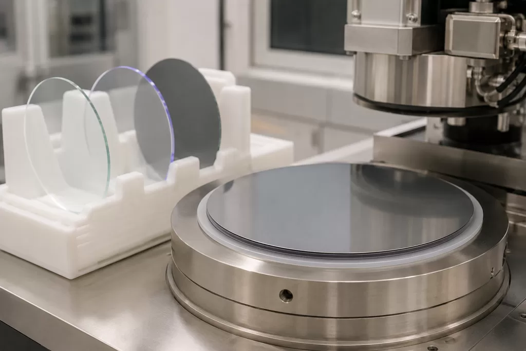
1. What Is a Temporary Wafer Carrier?
A temporary wafer carrier is a rigid substrate bonded to the front side of a device wafer using a removable adhesive or release-layer system.
The carrier supports the device wafer during processes such as:
- Back grinding and wafer thinning
- Chemical mechanical polishing
- Backside lithography
- Dry and wet etching
- Metal deposition and plating
- Through-silicon via processing
- Redistribution layer formation
- Cleaning and inspection
- Thin-wafer transportation between tools
After backside processing is completed, the device wafer is separated from the carrier and transferred to a film frame, permanent substrate or subsequent packaging process.
This is different from a FOUP, wafer cassette or transport tray. A temporary carrier is physically bonded to the wafer and remains part of the wafer stack during processing.
Industry process guidance describes temporary bonding as reversibly mounting a device wafer to a carrier with a polymeric or inorganic bonding system. The carrier and bonding material work together to provide mechanical support during thinning and backside processing. Brewer Science
2. Why Carrier Material Selection Matters
The carrier affects more than mechanical support. Its properties influence the entire temporary bonding and debonding process.
Important selection factors include:
- Device wafer material
- Original and final wafer thickness
- Wafer diameter or panel dimensions
- Maximum process temperature
- Number and severity of thermal cycles
- Grinding and polishing forces
- Wet and dry process chemistries
- Device-side topography and bump height
- Bonding adhesive or release-layer system
- Debonding method and laser wavelength
- Required alignment accuracy
- Tool chucking and wafer-detection compatibility
- Carrier reuse and cleaning requirements
A carrier that is sufficiently rigid may still cause problems if its coefficient of thermal expansion does not match the device wafer. Likewise, a transparent carrier will not automatically support laser debonding unless its transmission range matches the laser wavelength and release-layer design.
Carrier material, adhesive, release layer and debonding equipment should therefore be selected as a complete process system.
3. Glass Temporary Wafer Carriers
Glass is currently one of the most widely used carrier materials for temporary bonding in wafer thinning, fan-out packaging and 2.5D/3D integration.
Advantages of Glass Carriers
Optical Transparency
Selected glass compositions transmit ultraviolet, visible or infrared light. This enables:
- Through-carrier alignment
- Optical inspection of the bond interface
- UV curing of bonding adhesives
- UV or laser-assisted debonding
- Detection of voids and bonding defects
Glass is particularly attractive when the release layer must be irradiated through the carrier.
Controlled Thermal Expansion
Different glass compositions can be engineered with different coefficients of thermal expansion. This allows the carrier to be better matched with silicon, molded packages or other device structures.
Commercial advanced-packaging glass carriers are available with tunable thermal and mechanical properties, low TTV and warp, optical transparency and semiconductor-compatible chemical durability. Corning
High Dimensional Precision
Precision glass carriers can be manufactured with controlled:
- Diameter
- Thickness
- Total thickness variation
- Flatness
- Bow and warp
- Edge profile
- Surface roughness
A uniform carrier helps maintain consistent bond-line thickness and grinding results across the wafer.
Limitations of Glass Carriers
Glass is brittle and can be sensitive to edge damage, scratches and localized mechanical impact. Its stiffness, thermal conductivity and fracture behavior also vary with composition and thickness.
Some semiconductor tools are designed specifically for silicon wafers. Transparent glass may require modified wafer sensors, electrostatic chucks, edge handling or backside coatings.
Glass is generally a strong choice when optical access and laser debonding are important, but equipment compatibility must be confirmed before implementation.
4. Sapphire Temporary Wafer Carriers
Sapphire is a single-crystal aluminum oxide material that combines optical transparency with exceptionally high hardness, rigidity and chemical resistance.
Advantages of Sapphire Carriers
High Rigidity
Sapphire has substantially higher stiffness than most carrier glasses. This helps suppress carrier bending under grinding pressure and can improve wafer-stack stability during demanding mechanical processes.
The actual wafer-stack deformation, however, still depends on carrier thickness, device wafer thickness, adhesive properties and thermal stress.
High Hardness and Wear Resistance
Sapphire resists scratching, abrasion and repeated mechanical contact. This can be valuable when carriers are cleaned, inspected and reused for multiple process cycles.
Its wear resistance also helps preserve the carrier surface and edge geometry during repeated handling.
Thermal and Chemical Stability
Sapphire performs well in elevated-temperature, corrosive and plasma-processing environments. It is electrically insulating and has useful thermal conductivity compared with many glasses.
Sapphire material suppliers identify high rigidity, abrasion resistance, heat resistance, corrosion resistance and optical transmission as its principal engineering advantages. Kyocera
Optical Access
Sapphire transmits across a broad optical range, depending on crystal quality, thickness, surface finish and wavelength. It can support optical inspection and selected laser-based release processes.
The sapphire orientation and the laser wavelength must be specified because optical and thermal properties can vary with crystal direction.
Limitations of Sapphire Carriers
Sapphire is generally more expensive than standard glass or silicon carriers. Its high hardness also makes cutting, edge finishing, drilling and precision machining more difficult.
Other points to evaluate include:
- Crystal orientation
- Direction-dependent thermal expansion
- Surface quality requirements
- Edge strength
- Adhesive compatibility
- Laser wavelength transmission
- Cleaning method
- Reuse expectations
High rigidity is not automatically beneficial in every process. If thermal expansion mismatch is significant, a very rigid carrier can transfer stress into the device wafer or bonding layer rather than absorbing it.
Sapphire is most suitable when high rigidity, wear resistance, chemical durability and optical access are all important enough to justify the additional material and processing cost.
5. Silicon Temporary Wafer Carriers
Silicon carriers are commonly considered when the device wafer is also silicon or when the production line is optimized around standard silicon wafer handling.
Advantages of Silicon Carriers
Thermal Expansion Compatibility
A silicon carrier generally provides a close thermal expansion match with a silicon device wafer. This can reduce thermally induced stress during heating, cooling and repeated process cycles.
It is especially useful when dimensional stability and lithographic alignment must be maintained across multiple temperature steps.
Semiconductor Equipment Compatibility
Silicon carriers are usually compatible with standard:
- Vacuum chucks
- Electrostatic chucks
- Robotic end effectors
- Wafer sensors
- Alignment systems
- Edge-grip handling equipment
This reduces the need to modify equipment originally designed for silicon substrates.
Established Wafer Specifications
Silicon carriers are available in standard wafer diameters, crystal orientations, thicknesses, surface finishes and edge profiles. Double-side-polished silicon may also be selected when backside flatness or infrared optical access is required.
IR Debonding Options
Silicon does not transmit visible or UV light, but it can transmit selected infrared wavelengths. Specialized systems combine silicon carriers with infrared lasers and compatible release layers.
EV Group describes IR laser debonding systems that transmit a selected IR wavelength through a silicon carrier and activate an inorganic release layer. The same source notes that silicon carriers can improve compatibility with semiconductor equipment originally designed around silicon. EV Group
Limitations of Silicon Carriers
Silicon cannot be used for conventional UV through-carrier debonding. Optical inspection through the carrier also requires suitable infrared equipment.
Other considerations include:
- Silicon carrier thickness
- Resistivity and conductivity
- Front- and backside surface finish
- Particle and metal contamination control
- Edge exclusion
- Bow and warp
- IR wavelength compatibility
- Release-layer design
- Carrier breakage during mechanical debonding
A silicon carrier is often the most practical option when equipment compatibility, thermal matching and standard wafer handling are more important than visible or UV transparency.
6. Glass vs. Sapphire vs. Silicon Carrier Comparison
| Selection Factor | Glass Carrier | Sapphire Carrier | Silicon Carrier |
|---|---|---|---|
| Optical access | Excellent, depending on glass composition | Excellent across a broad wavelength range | Limited mainly to selected IR wavelengths |
| UV through-carrier debonding | Commonly suitable | Potentially suitable with matched wavelength | Generally unsuitable |
| IR debonding | Possible with suitable glass and release layer | Possible with suitable wavelength | Possible with specialized IR release systems |
| Mechanical rigidity | Moderate to high, depending on composition and thickness | Very high | High |
| Wear resistance | Moderate | Excellent | Moderate |
| CTE matching | Tunable through glass composition | Must consider crystal orientation and device material | Excellent match for silicon device wafers |
| Chemical durability | Good to excellent, depending on glass | Excellent | Good under compatible chemistries |
| Standard fab-tool compatibility | May require tool adjustment | May require tool adjustment | Generally excellent |
| Machining cost | Moderate | High | Moderate |
| Typical applications | Fan-out packaging, laser debonding, optical alignment | High-stability processing, repeated use, harsh environments | Silicon wafer processing, IR debonding, fab-compatible flows |
7. Matching the Carrier to the Debonding Method
The debonding method often determines the appropriate carrier material.
UV Laser Debonding
UV laser debonding normally requires a UV-transparent carrier and a release layer that absorbs or decomposes under the selected laser wavelength.
Glass is widely used for this process. Sapphire may also be considered, but transmission and release-layer compatibility must be verified.
IR Laser Debonding
IR debonding may use glass, sapphire or silicon, depending on the wavelength and release-layer system.
Silicon carrier solutions require carefully selected IR wavelengths because transmission changes significantly with wavelength, doping and wafer thickness.
Thermal Slide Debonding
Thermal slide debonding softens the temporary adhesive at an elevated temperature, allowing the carrier and device wafer to move laterally relative to each other.
Glass, sapphire and silicon can all be considered, provided that:
- The carrier remains dimensionally stable
- The adhesive reaches the required release condition
- The device structure tolerates the debonding temperature
- Sliding forces do not damage the thin wafer
Mechanical Debonding
Mechanical separation may be suitable for certain adhesive and carrier systems but must be carefully controlled. Excessive peel, lift or bending stress can crack a thin wafer or damage low-k materials and fragile device structures.
Chemical Debonding
Chemical release requires compatibility between the carrier, adhesive, release layer and solvent. The process must also prevent solvent penetration into sensitive device structures.
Modern temporary bonding platforms may support thermal, mechanical, UV-laser or IR-laser separation, but the carrier and adhesive must be qualified together. EV Group
8. Critical Carrier Specifications
A carrier-wafer inquiry should include more than material and diameter.
Recommended specifications include:
- Carrier material and material grade
- Wafer diameter or panel dimensions
- Carrier thickness and tolerance
- Total thickness variation
- Bow and warp limits
- Surface flatness
- Frontside and backside surface roughness
- Edge profile and edge exclusion
- Notch or flat dimensions
- Crystal orientation for sapphire or silicon
- Optical transmission wavelength
- Maximum process temperature
- Required chemical resistance
- Device wafer material
- Device wafer starting and final thickness
- Maximum frontside topography or bump height
- Temporary bonding material
- Debonding method
- Laser wavelength and energy range
- Required carrier reuse cycles
- Cleaning and contamination specifications
- Packaging and particle-control requirements
For laser debonding, a general statement such as “transparent carrier required” is insufficient. The inquiry should specify the actual wavelength and required transmission range.
9. Common Carrier Selection Mistakes
Selecting the Carrier Without the Adhesive
Carrier performance depends heavily on bond-line adhesion, adhesive thickness uniformity, thermal stability and release behavior.
A strong carrier cannot compensate for an adhesive that delaminates during grinding or leaves excessive residue after debonding.
Evaluating Only Room-Temperature Flatness
A carrier may be flat during incoming inspection but develop bow during heating because of CTE mismatch within the bonded stack.
Thermal-cycle testing is therefore more meaningful than room-temperature flatness alone.
Ignoring Equipment Detection
Transparent carriers may not be reliably detected by sensors designed for opaque silicon wafers. Chucking, alignment and robotic handling should be verified before production qualification.
Assuming All Transparent Materials Support the Same Laser
Glass and sapphire transmission varies with wavelength, thickness, impurities and surface treatment. The complete optical stack—including the carrier, adhesive and release layer—must be tested.
Focusing Only on Carrier Price
Carrier cost should be evaluated together with:
- Wafer breakage rate
- Grinding uniformity
- Debond yield
- Carrier cleaning
- Number of reuse cycles
- Equipment modification
- Process throughput
- Adhesive residue removal
A more expensive carrier may have a lower total cost when it reduces breakage or supports repeated reuse.
10. How to Choose the Right Temporary Carrier
Choose a glass carrier when:
- UV or visible optical access is required
- Laser debonding must occur through the carrier
- CTE must be adjusted through glass composition
- Fan-out wafer or panel-level packaging is involved
- Low TTV and optical inspection are priorities
Choose a sapphire carrier when:
- Very high rigidity is required
- The carrier will experience repeated mechanical contact
- High wear and chemical resistance are important
- Optical access and dimensional stability are both needed
- Carrier reuse can justify the higher initial cost
Choose a silicon carrier when:
- The device wafer is silicon
- Existing fab equipment is optimized for silicon
- Thermal expansion matching is a major concern
- Visible or UV transparency is unnecessary
- A compatible IR release system is available
Conclusion
Glass, sapphire and silicon can all serve as effective temporary wafer carriers, but they solve different process problems.
Glass provides optical access, tunable thermal properties and established compatibility with UV or laser debonding. Sapphire offers exceptional rigidity, wear resistance and stability for demanding processing environments. Silicon provides close thermal matching with silicon device wafers and strong compatibility with standard semiconductor equipment.
The correct choice should be based on the complete wafer-stack process rather than a single material property. Device wafer thickness, process temperature, grinding force, chemistry, tool compatibility, adhesive behavior and debonding method must all be evaluated together.
A properly specified carrier reduces wafer breakage, controls warpage, improves backside processing uniformity and supports reliable handling of ultra-thin wafers throughout advanced semiconductor manufacturing.