
Wafer Dicing Saw Selection Guide: Blade Dicing vs Laser vs Water-Guided Laser for Silicon, SiC, Glass and HBM
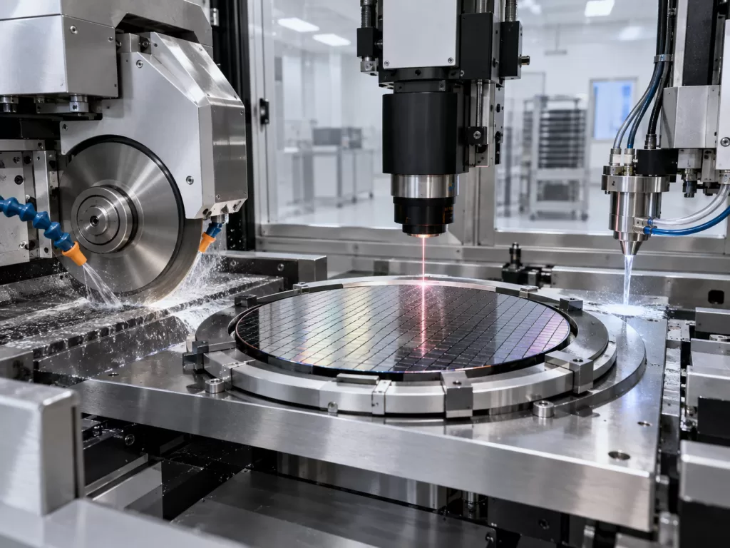
Wafer dicing is the final separation step that converts a processed semiconductor wafer into individual dies. At first glance, the objective appears simple: cut along the dicing streets without damaging the devices. In practice, wafer singulation has become increasingly difficult. Modern semiconductor manufacturing involves thinner silicon wafers, hard and brittle SiC substrates, glass wafers, backside […]
Temporary Wafer Carrier Selection Guide: Glass, Sapphire and Silicon Carriers for Thin-Wafer Grinding, Bonding and Debonding
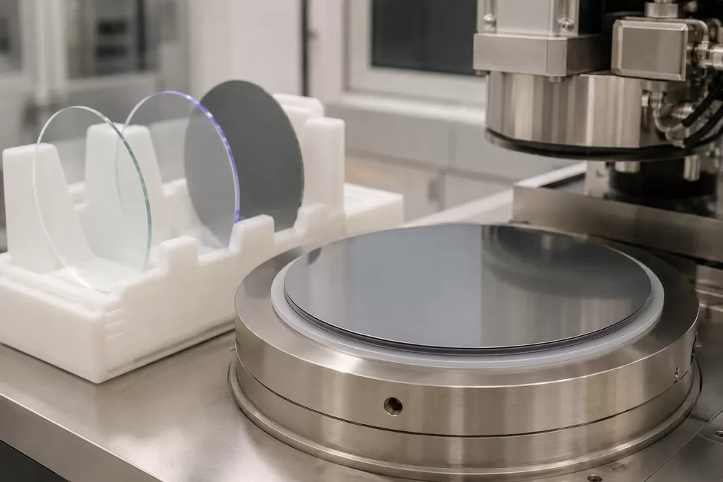
As semiconductor wafers become thinner, larger and more structurally complex, maintaining mechanical stability throughout manufacturing becomes increasingly difficult. Ultra-thin silicon, SiC, GaN, MEMS and compound semiconductor wafers may crack, warp, chip or deform during back grinding, polishing, lithography, deposition and wet processing. A temporary wafer carrier provides the rigid support required to process these fragile […]
Glass Wafer Edge Quality Requirements for Advanced Packaging Applications
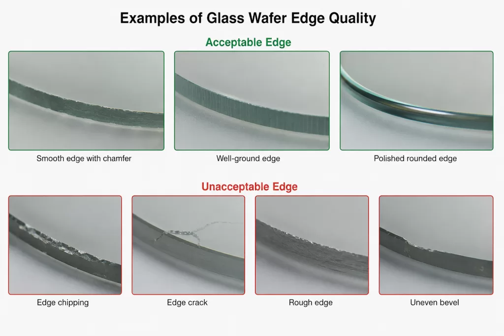
Glass wafers are increasingly used in advanced semiconductor packaging as carrier wafers, interposers, through-glass-via substrates, MEMS packaging substrates and temporary bonding platforms. Their dimensional stability, electrical insulation, optical transparency and adjustable coefficient of thermal expansion make them suitable for fan-out packaging, 2.5D and 3D integration, RF modules and heterogeneous integration. However, the performance of a […]
TGV Sapphire Substrate: Material Principles, Microstructure Design, and Advanced Packaging Applications
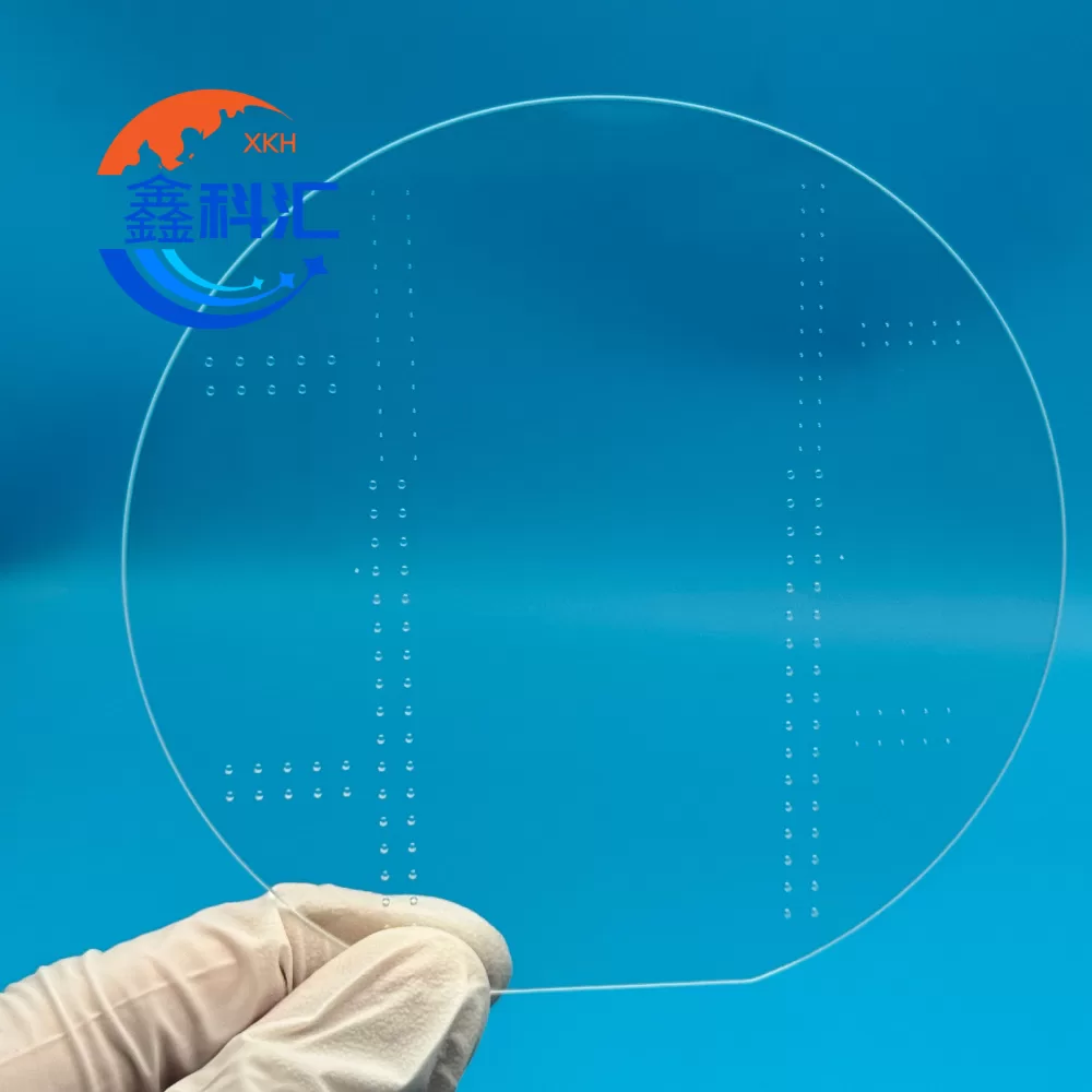
In advanced semiconductor packaging, MEMS devices, optical sensors, and high-frequency electronic systems, device structures are gradually moving from traditional two-dimensional layouts toward three-dimensional integration. To achieve shorter signal paths, higher integration density, and more compact device architectures, vertical interconnection technologies have become increasingly important. One important concept in this field is TGV, which stands for […]
Silicon Carbide (SiC): The Enabling Material for AI Chip Packaging and Next-Generation Server Power Systems
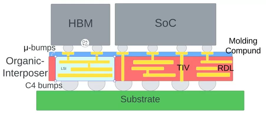
With the rapid expansion of artificial intelligence workloads, both data centers and advanced semiconductor devices are facing unprecedented challenges in power consumption and thermal management. Leading platforms from companies such as Intel and NVIDIA are pushing system power levels to new extremes. Server racks are moving from tens of kilowatts to over 100 kW, while […]
Technical Breakthrough and Industry Prospects of 14-Inch SiC Substrates

Silicon carbide (SiC), a third-generation semiconductor material, has attracted significant attention due to its wide bandgap, high breakdown electric field, and superior thermal conductivity. These properties make SiC a critical material for high-power electronic devices in electric vehicles (EVs), data centers, renewable energy systems, and other high-performance applications. In recent years, the wafer size of […]
The Savior of AI Chip Thermal Management: Why NVIDIA’s Next-Gen GPUs are Switching to Silicon Carbide (SiC) Interposers
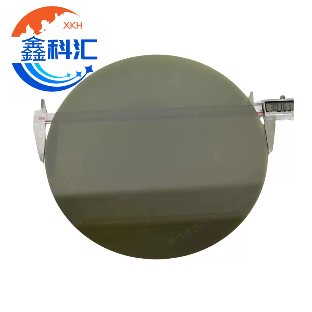
In the rapidly evolving landscape of high-performance computing (HPC), we are witnessing a transition from the era of “Silicon for everything” to an era of “Specialized Materials for Performance.” As NVIDIA prepares to unleash its next-generation Rubin architecture, a quiet but seismic shift is happening beneath the silicon dies. To overcome the physical limits of […]
Global Semiconductor Supply Chain Shifts to Mainland China: 2025 Opportunities for Material Localization
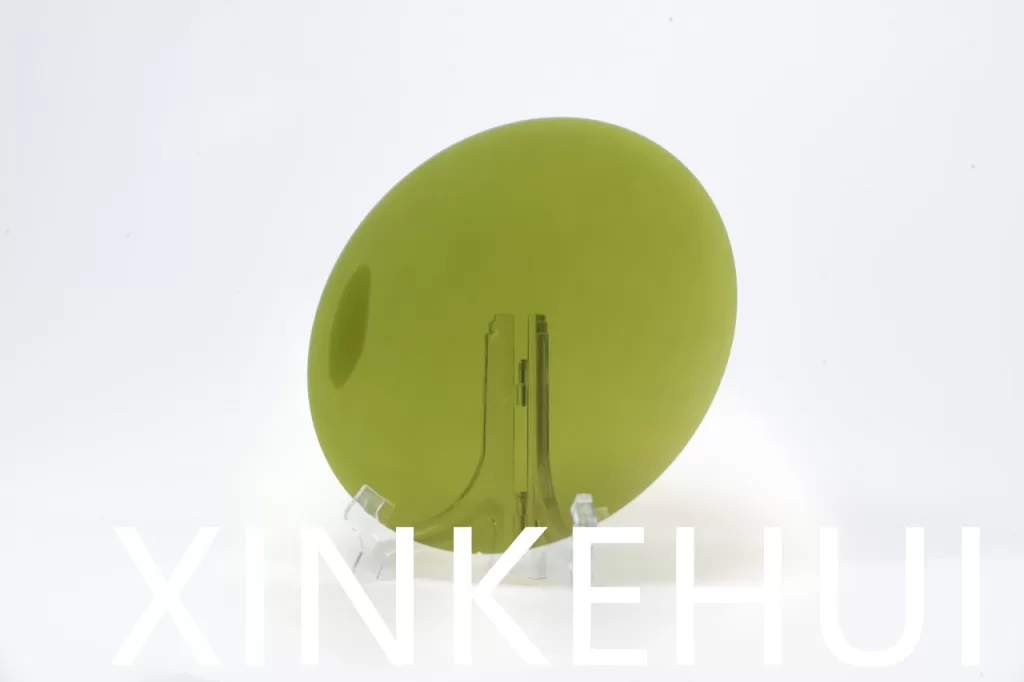
In recent years, the global semiconductor supply chain has been undergoing a major structural shift. Manufacturing, assembly, and many upstream segments continue to move toward mainland China. By 2025, driven by expanding advanced process demand, regional supply chain restructuring, and changing global policy environments, mainland China has become one of the fastest-growing semiconductor manufacturing hubs […]