
Wafer dicing is the final separation step that converts a processed semiconductor wafer into individual dies.
At first glance, the objective appears simple: cut along the dicing streets without damaging the devices.
In practice, wafer singulation has become increasingly difficult.
Modern semiconductor manufacturing involves thinner silicon wafers, hard and brittle SiC substrates, glass wafers, backside metallization, dielectric layers, temporary bonding materials and increasingly narrow streets between adjacent dies.
HBM and other advanced packaging technologies add further challenges because the individual dies can be extremely thin and mechanically fragile.
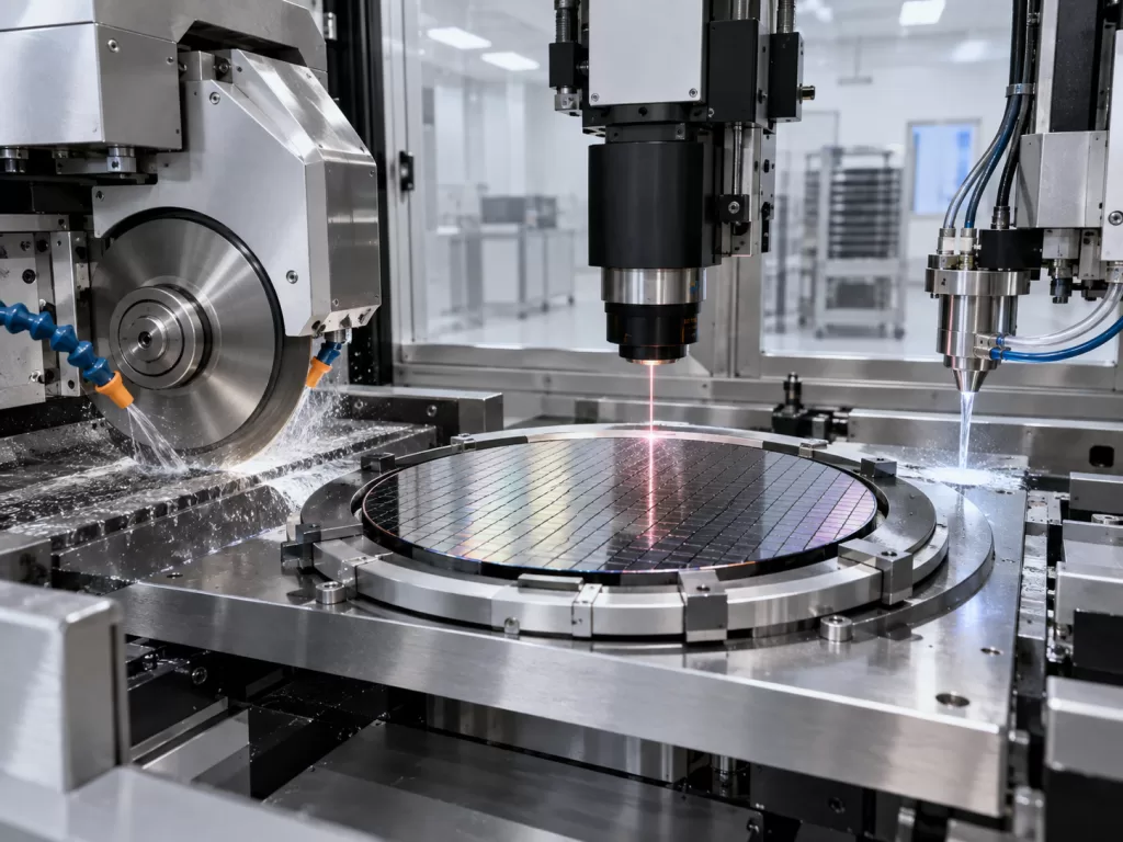
As a result, selecting a wafer dicing saw is no longer simply a choice of blade diameter or spindle speed.
Manufacturers increasingly need to compare three major processing approaches:
- blade dicing
- conventional or ultrafast laser dicing
- water-guided laser dicing
Each technology has advantages and limitations depending on wafer material, thickness, device structure, edge-quality requirements and production economics.
This guide compares these technologies for silicon, SiC, glass and advanced packaging applications.
Why Wafer Dicing Technology Matters
Dicing quality directly affects die yield and downstream packaging reliability.
Poor singulation can introduce defects such as:
- edge chipping
- backside chipping
- microcracks
- delamination
- metal peeling
- thermal damage
- recast material
- debris contamination
- reduced die fracture strength
- excessive kerf width
Some defects are visible immediately after cutting.
Others remain as subsurface damage and may lead to die failure during die attach, wire bonding, molding, thermal cycling or long-term device operation.
The best dicing method therefore depends on more than cutting speed.
A practical selection process should consider:
- wafer material
- wafer thickness
- dicing street width
- backside layers
- required die strength
- allowable heat-affected zone
- particle and water sensitivity
- throughput
- consumable cost
- automation requirements
1. Blade Dicing: The Established Semiconductor Standard
Blade dicing is the most established mechanical wafer singulation method.
A high-speed spindle rotates a thin diamond blade while the wafer is moved accurately along predetermined dicing streets.
Cooling water is normally supplied during cutting to control temperature and remove debris.
Blade dicing has been used for decades for semiconductor wafers and remains highly relevant because of its mature equipment ecosystem and relatively straightforward process control.
Advantages of Blade Dicing
Mature and Proven Technology
Blade dicing equipment, blades, mounting tapes and process recipes are widely available.
For conventional silicon wafers with sufficient street width, the process is highly mature.
Competitive Processing Cost
For high-volume production of suitable materials, blade dicing can provide an attractive cost per wafer.
The equipment and consumable structure is well understood, making production planning comparatively predictable.
High Throughput for Conventional Silicon
Standard silicon wafers with adequate thickness and conventional device structures can often be diced efficiently with optimized blades.
Wide Range of Blade Specifications
Blade composition, grit size, bond type, thickness and exposure can be adjusted according to the wafer material and cutting requirement.
This makes blade dicing more flexible than its relatively simple operating principle might suggest.
Limitations of Blade Dicing
The main disadvantage is that the blade physically contacts the wafer.
This generates mechanical forces.
For thick and mechanically robust silicon wafers, these forces can often be managed successfully.
For ultra-thin wafers, fragile low-k structures or hard brittle materials, mechanical stress becomes more significant.
Potential problems include:
- front-side chipping
- backside chipping
- lateral cracks
- edge damage
- blade wear
- die cracking
- metal-layer peeling
Another limitation is kerf width.
The blade itself has a physical width, so the dicing street must provide sufficient space for the cut and process tolerance.
As chip manufacturers attempt to obtain more dies from each wafer, reducing street width becomes increasingly valuable.
2. Laser Dicing: Non-Contact Wafer Singulation
Laser dicing replaces the mechanical blade with a focused laser beam.
Depending on the process, the laser may remove material directly from the wafer surface or create modified regions inside the wafer that later allow controlled separation.
Several laser approaches exist, including:
- laser ablation
- laser grooving
- laser full-cut dicing
- stealth dicing
- nanosecond laser processing
- picosecond laser processing
- femtosecond laser processing
The correct laser source depends strongly on the optical and thermal properties of the wafer material.
Advantages of Laser Dicing
No Mechanical Blade Contact
Because the laser does not require a rotating blade to mechanically grind through the wafer, mechanical cutting forces can be significantly reduced.
This is attractive for thin and fragile wafers.
Narrower Kerf Potential
A focused laser beam can create a narrower processing path than many conventional blade processes.
Narrower streets can contribute to improved wafer utilization.
Suitable for Hard and Brittle Materials
Laser processing can be particularly useful for materials that are difficult to cut mechanically.
Examples include:
- silicon carbide
- sapphire
- gallium nitride
- glass
- compound semiconductor wafers
Flexible Process Control
Laser power, wavelength, pulse duration, repetition rate, scanning speed and focal position can all be adjusted.
This gives engineers substantial control over how energy interacts with the wafer.
Limitations of Conventional Laser Dicing
Laser processing introduces a different set of challenges.
Instead of mechanical damage, engineers must control thermal effects.
Depending on the laser and process parameters, potential defects include:
- heat-affected zones
- melted material
- recast layers
- redeposition
- microcracks
- surface debris
- changes in die fracture strength
Shorter pulse lasers can reduce the amount of heat transferred into the surrounding material.
However, ultrafast laser equipment also increases equipment complexity and investment cost.
Laser dicing therefore should not automatically be considered superior to blade dicing.
The correct process is determined by the actual wafer structure and quality requirements.
3. Stealth Dicing for Thin and Brittle Wafers
Stealth dicing differs from conventional surface ablation.
Instead of removing material along the entire cutting path, a focused laser is directed inside a material that is sufficiently transparent at the selected wavelength.
The laser creates an internal modified layer.
The wafer is subsequently separated by expanding the dicing tape or applying controlled mechanical force.
Because the process does not necessarily create an open surface kerf during laser irradiation, stealth dicing can reduce some of the debris and surface damage associated with conventional cutting.
It is particularly attractive where:
- narrow streets are required
- wafers are thin
- surface contamination must be minimized
- mechanical chipping must be reduced
Stealth dicing has been applied to semiconductor and brittle substrate processing, including silicon and SiC under suitable conditions.
However, internal laser focusing, wafer material properties and device-layer structure must all be considered before selecting the process.
4. What Is Water-Guided Laser Dicing?
Water-guided laser dicing combines laser energy with a very fine water jet.
Rather than simply spraying cooling water around a conventional laser process, the laser beam is coupled into a narrow water jet.
The water jet acts as an optical guide that carries the laser energy toward the workpiece.
This approach combines several characteristics of laser machining and water-assisted processing.
The water can help:
- cool the cutting zone
- reduce thermal accumulation
- remove processing debris
- protect the surrounding surface
- maintain a relatively long effective working distance
- reduce some forms of redeposition
This makes water-guided laser technology particularly interesting for hard, brittle or thermally sensitive materials.
Water-Guided Laser vs Conventional Laser
A conventional focused laser typically reaches its highest energy density around a limited focal region.
A water-guided laser transports the beam through the water jet.
This changes the way the laser interacts with the substrate and can provide process advantages for certain geometries and materials.
However, water-guided laser systems are more specialized.
Equipment investment, process integration and application experience therefore become important considerations.
They should not be viewed as a universal replacement for either blade or conventional laser dicing.
Blade vs Laser vs Water-Guided Laser
| Factor | Blade Dicing | Laser Dicing | Water-Guided Laser |
|---|---|---|---|
| Cutting mechanism | Mechanical grinding | Laser-material interaction | Laser guided by fine water jet |
| Mechanical stress | Higher | Very low | Very low |
| Thermal influence | Low | Depends strongly on laser/process | Generally easier to control |
| Kerf potential | Moderate | Narrow | Narrow |
| Chipping risk | Material dependent | Generally reduced | Can be low |
| Debris | Slurry and particles | Ablation debris possible | Water assists debris removal |
| Consumables | Diamond blade | Lower direct cutting-tool wear | Specialized nozzles/system maintenance |
| Silicon suitability | Excellent | Excellent for selected structures | Application dependent |
| SiC suitability | Possible but difficult | Strong candidate | Strong candidate for selected processes |
| Glass suitability | Possible with optimized process | Strong candidate | Strong candidate |
| Ultra-thin wafers | Increasingly challenging | Attractive | Potentially attractive |
| Capital cost | Mature/moderate | Higher | Typically higher/specialized |
| Process maturity | Very high | High and growing | More specialized |
The table should be treated as a general engineering comparison rather than a universal ranking.
Actual results depend heavily on equipment configuration and wafer design.
Dicing Silicon Wafers
Silicon remains the most common semiconductor wafer material.
For conventional silicon wafers, blade dicing remains an extremely practical solution.
If the wafer has:
- sufficient thickness
- reasonable street width
- manageable metal structures
- standard backside conditions
a properly optimized blade process can provide good productivity and acceptable edge quality.
However, silicon wafers are becoming thinner.
Advanced power devices, stacked packages and memory products increasingly require thin dies.
As thickness decreases, mechanical integrity also decreases.
The relative importance of:
- backside chipping
- die strength
- blade loading
- edge cracking
therefore increases.
Laser processing becomes more attractive when conventional blade dicing approaches its limits.
Dicing Ultra-Thin Silicon
Ultra-thin silicon requires special attention because a process that works well for a standard wafer may produce unacceptable damage after aggressive back grinding.
Potential solutions include:
- optimized thin blades
- multi-step blade cutting
- laser grooving followed by blade dicing
- laser full-cut processing
- stealth dicing
- hybrid processes
The correct method depends on whether the wafer also contains:
- backside metal
- die attach film
- redistribution layers
- low-k dielectric structures
- temporary bonding layers
This is particularly relevant in advanced packaging.
Dicing Silicon Carbide Wafers
SiC presents a very different challenge.
Silicon carbide is extremely hard and brittle.
These properties are beneficial for power semiconductor operation but make wafer processing more difficult.
Mechanical blade dicing of SiC is possible, but compared with silicon it can result in:
- faster blade wear
- lower feed speed
- higher cutting forces
- increased chipping risk
- higher consumable cost
Process optimization therefore becomes important.
Why Laser Dicing Is Attractive for SiC
Laser processing removes the dependence on continuous mechanical grinding.
This can reduce mechanical loading on the wafer and eliminate some of the blade-wear limitations associated with SiC.
Possible approaches include:
- laser scribing
- laser ablation
- ultrafast laser dicing
- stealth-type internal modification
- water-guided laser processing
However, SiC laser processing is not automatically simple.
The laser wavelength, pulse duration and energy density must be selected carefully.
Excessive energy can still create thermal damage or undesirable surface morphology.
Water-Guided Laser for SiC
Water-guided laser processing can be especially interesting for SiC because the water assists both thermal management and debris removal.
Potential advantages include:
- low mechanical stress
- reduced blade consumption
- controlled heat input
- improved debris removal
- potential for high-quality edges
For expensive SiC wafers, minimizing kerf loss and die damage can be economically important.
However, production throughput, equipment cost and process repeatability must be evaluated against optimized blade and conventional laser alternatives.
Dicing Glass Wafers
Glass is increasingly relevant to semiconductor manufacturing.
Applications include:
- glass carrier wafers
- temporary bonding carriers
- MEMS
- optical devices
- wafer-level packaging
- glass interposers
- through-glass-via substrates
Glass introduces two major dicing challenges:
- brittleness
- crack propagation
Mechanical blade cutting can generate edge chips and microcracks if blade, feed speed, coolant flow and support conditions are not optimized.
Laser processing provides an alternative.
Ultrafast lasers can create highly localized energy deposition with reduced thermal impact compared with longer-pulse processing.
Depending on glass composition and thickness, processes may include:
- laser scribing and breaking
- laser ablation
- filamentation
- stealth-type internal modification
- water-assisted laser processing
Water-Guided Laser for Glass
Water-guided lasers can be suitable for certain glass machining applications because the cooling effect helps control heat accumulation while the water removes debris.
For semiconductor glass components, engineers may prioritize:
- edge quality
- crack depth
- particle contamination
- kerf width
- dimensional accuracy
The optimum process depends strongly on glass composition.
Borosilicate glass, fused silica and specialized semiconductor glass may respond differently to the same laser parameters.
Therefore, a process developed for one glass family should not automatically be transferred to another.
Wafer Dicing for HBM and Advanced Packaging
High Bandwidth Memory places particularly demanding requirements on wafer thinning and die handling.
HBM achieves high bandwidth by vertically stacking multiple memory dies.
The individual dies must therefore be thin enough to support the required package architecture.
As die thickness decreases, singulation becomes increasingly sensitive to mechanical and thermal damage.
Important concerns include:
- ultra-thin silicon
- die fracture strength
- narrow streets
- backside damage
- warpage
- temporary bonding
- backside metal
- die attach film
- high-value device wafers
A small improvement in dicing quality can become important when the die will later undergo stacking and bonding processes.
Is Laser Dicing Better for HBM?
There is no single universal answer.
For thin memory wafers, laser dicing offers attractive characteristics because it can reduce mechanical loading and enable narrow processing streets.
However, the final process depends on wafer architecture.
A manufacturer may use:
Laser grooving + blade dicing
The laser first removes fragile upper dielectric or metal structures, while a blade completes the bulk silicon cut.
Laser full cut
The laser performs complete singulation for suitable thin wafer structures.
Stealth dicing
Internal modification enables separation while reducing surface material removal.
Optimized blade dicing
Blade dicing can remain competitive if wafer thickness, street width and device structure allow it.
The correct HBM singulation solution should therefore be selected as part of the complete wafer-thinning and packaging flow rather than as an isolated process.
Can Water-Guided Laser Be Used for HBM?
Potentially, but it should be evaluated application by application.
Water-guided laser processing offers features that may be attractive for advanced packaging:
- low mechanical cutting force
- efficient local cooling
- reduced thermal accumulation
- narrow cutting capability
- effective debris removal
However, HBM manufacturing requires extremely high productivity and process stability.
Integration with:
- device structures
- dicing tape
- backside films
- contamination requirements
- downstream die handling
must be validated.
For this reason, water-guided laser should be considered an engineering option rather than automatically described as the standard HBM dicing process.
Hybrid Dicing Is Becoming Increasingly Important
The semiconductor industry does not always have to choose between blade and laser.
Hybrid processes can combine their strengths.
A common concept is:
laser grooving + blade cutting
The laser removes sensitive layers around the dicing street.
The mechanical blade then cuts the remaining silicon.
This approach can help reduce problems such as:
- low-k dielectric delamination
- metal peeling
- surface chipping
while retaining the productivity advantages of mechanical cutting through the bulk wafer.
As wafer structures become increasingly complex, hybrid dicing is likely to remain important.
How to Select a Wafer Dicing Saw
Before selecting equipment, manufacturers should provide complete wafer information.
1. Wafer Material
Specify whether the wafer is:
- silicon
- SiC
- sapphire
- GaAs
- GaN
- glass
- ceramic
- another brittle substrate
Material hardness and optical absorption strongly influence process selection.
2. Wafer Diameter
Typical equipment requirements may involve:
- 100mm
- 150mm
- 200mm
- 300mm
Equipment handling architecture changes significantly with wafer diameter.
3. Wafer Thickness
Wafer thickness is one of the most important parameters.
A method suitable for a 700 μm wafer may not be appropriate for a wafer thinned below 100 μm.
4. Dicing Street Width
Narrow streets increasingly favor technologies capable of reducing kerf.
This can become especially important for high-value semiconductor wafers.
5. Device Structure
Provide information about:
- metal layers
- passivation
- low-k materials
- redistribution layers
- TSV structures
- backside coatings
- die attach film
The wafer is rarely simply a piece of bare silicon.
6. Required Edge Quality
Critical specifications may include:
- front-side chipping
- backside chipping
- sidewall roughness
- crack depth
- die fracture strength
These requirements can determine whether blade, laser or hybrid processing is most appropriate.
7. Throughput
A technically excellent process is not automatically a commercially viable process.
Manufacturers must compare:
- wafers per hour
- die per wafer
- maintenance intervals
- blade replacement
- laser processing time
- equipment utilization
8. Cost per Wafer
The equipment purchase price is only one element.
Total dicing cost can include:
- blades
- water
- laser maintenance
- filters
- tape
- process yield
- damaged dies
- downtime
- labor
- preventive maintenance
For high-value SiC or advanced packaging wafers, improved yield can justify a more expensive dicing process.
Which Dicing Technology Should You Choose?
For conventional silicon wafers with generous dicing streets and mature process requirements:
Blade dicing remains a strong choice.
For thin silicon, brittle substrates or narrow streets:
Laser dicing becomes increasingly attractive.
For SiC, glass and other difficult materials where both thermal and mechanical damage must be controlled:
Ultrafast laser or water-guided laser technology deserves evaluation.
For HBM and advanced packaging:
Laser, blade and hybrid processes should be compared using the actual device stack and wafer thickness rather than selecting a technology based on the substrate material alone.
There is no universally best wafer dicing saw.
The correct equipment is the one that provides the required combination of:
- cut quality
- die strength
- throughput
- kerf width
- contamination control
- process stability
- cost per good die
Conclusion
Wafer dicing technology is evolving as semiconductor wafers become thinner, harder and more structurally complex.
Blade dicing continues to provide mature, cost-effective production for many silicon applications.
Laser dicing provides non-contact processing, narrower kerf potential and greater flexibility for thin or brittle materials.
Water-guided laser technology adds active cooling and debris removal to laser machining, making it an interesting option for materials such as SiC and glass.
For advanced packaging and HBM, the decision becomes even more application-specific.
Instead of asking simply whether blade or laser dicing is better, semiconductor manufacturers should evaluate the complete wafer structure, thickness, street width, quality requirement and production target.
A well-selected dicing process can reduce chipping and cracks, improve die strength, increase usable dies per wafer and ultimately lower the cost per qualified semiconductor device.