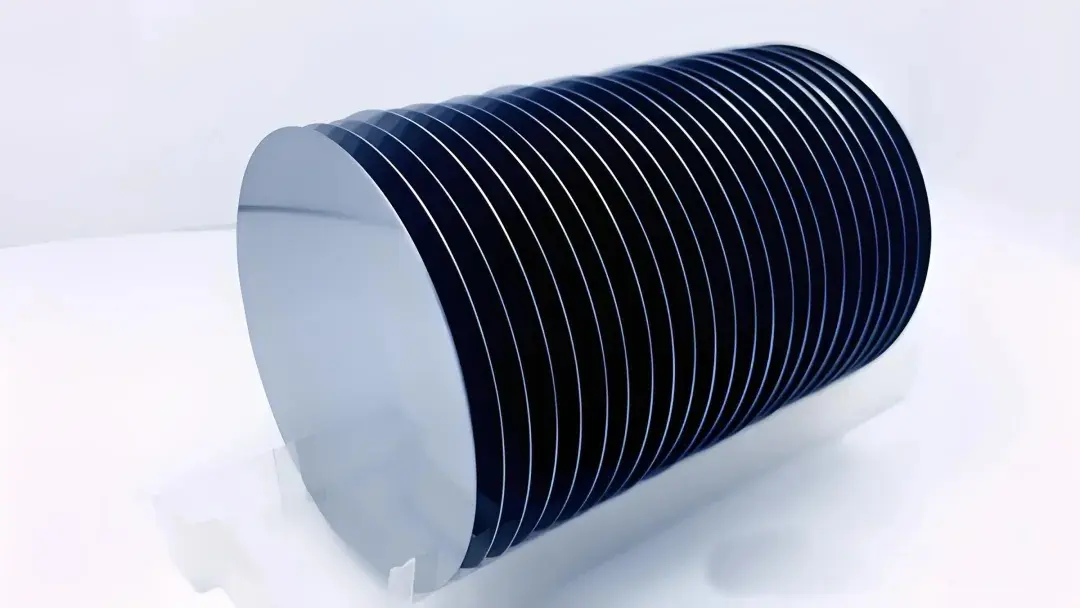
Why 300mm Silicon Wafers Matter for Advanced Semiconductor Production
The transition from 200mm to 300mm silicon wafers represents one of the most significant structural upgrades in the semiconductor manufacturing ecosystem. Beyond a simple increase
المورد الرائد عالمياً لمواد أشباه الموصلات
البريد الإلكتروني [email protected]
The transition from 200mm to 300mm silicon wafers represents one of the most significant structural upgrades in the semiconductor manufacturing ecosystem. Beyond a simple increase

1. Introduction: From Wafer Diameter to Industrial Capability In semiconductor technology, wafer diameter has historically served as a reliable indicator of manufacturing maturity. Each major

Silicon carbide (SiC) has rapidly moved from a niche material known only to semiconductor experts to a headline technology powering electric vehicles, renewable energy systems,
Silicon carbide (SiC) epitaxy is one of the most critical processes behind today’s high-voltage, high-frequency, and high-efficiency semiconductor devices. Although this thin crystalline layer is
The global shift toward electrification, renewable energy, and high-efficiency power electronics has brought silicon carbide (SiC) wafers into the spotlight. While SiC crystal growth and

Silicon wafers are essential components in modern electronics, serving as the foundation for devices ranging from smartphones and computers to solar panels and semiconductor devices.
In the fast-evolving world of semiconductors, silicon wafers are the foundation of almost all modern electronic devices—from smartphones and computers to medical devices and automotive