ニュース
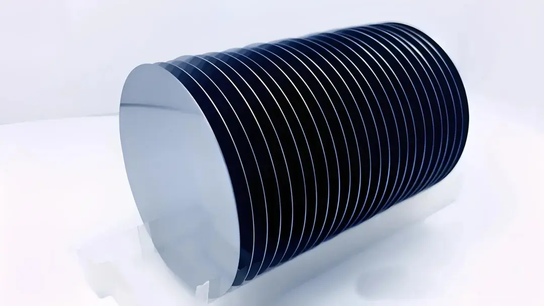
300mmウェーハの課題:大口径結晶成長の技術的ハードル(EFG vs. PVT)
Silicon carbide (SiC) has emerged as a cornerstone material for high-power electronics, electric vehicles, and next-generation semiconductor devices due to its exceptional thermal conductivity, high

Silicon carbide (SiC) has emerged as a cornerstone material for high-power electronics, electric vehicles, and next-generation semiconductor devices due to its exceptional thermal conductivity, high
炭化ケイ素(SiC)は、ニッチなワイドバンドギャップ材料から、次世代パワーエレクトロニクスの戦略的基盤へと急速に移行している。電気自動車への採用が加速する中,
The transition from 200mm to 300mm silicon wafers represents one of the most significant structural upgrades in the semiconductor manufacturing ecosystem. Beyond a simple increase
1. Introduction: From Wafer Diameter to Industrial Capability In semiconductor technology, wafer diameter has historically served as a reliable indicator of manufacturing maturity. Each major

炭化ケイ素(SiC)は、半導体の専門家だけが知っているニッチな材料から、電気自動車や再生可能エネルギー・システムに電力を供給する主要技術へと急速に移行した、,
炭化ケイ素(SiC)エピタキシーは、今日の高電圧、高周波、高効率半導体デバイスを支える最も重要なプロセスのひとつである。この薄い結晶層は
The global shift toward electrification, renewable energy, and high-efficiency power electronics has brought silicon carbide (SiC) wafers into the spotlight. While SiC crystal growth and