
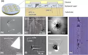
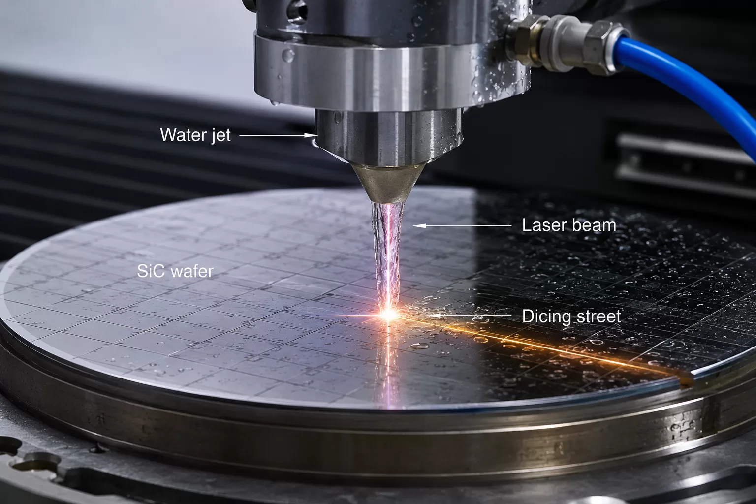
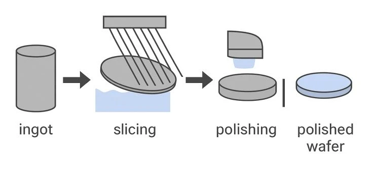
Výzvy při výrobě SiC destiček: růst krystalů, řezání a leštění
Silicon Carbide (SiC) has emerged as one of the most important semiconductor materials for next-generation power electronics. Thanks to its wide bandgap, high thermal conductivity,

Silicon Carbide (SiC) has emerged as one of the most important semiconductor materials for next-generation power electronics. Thanks to its wide bandgap, high thermal conductivity,

Silicon Carbide (SiC), as a third-generation wide-bandgap semiconductor material, has gained significant importance in power electronics, including electric vehicles, photovoltaic inverters, high-voltage power supplies, and

For years, silicon carbide (SiC) has been viewed primarily as a “new energy material” tied to electric vehicles, solar inverters, and industrial power electronics. But

Silicon carbide (SiC) wafers have become one of the most important wide-bandgap semiconductor substrates in power electronics, RF communication, and high-temperature applications. Among the most

1. Introduction In semiconductor manufacturing, a dummy wafer (also known as a monitor wafer or blank wafer) is a non-device-bearing wafer used to support and

1. Introduction The manufacturing of silicon carbide (SiC) power devices involves highly complex semiconductor processes, typically consisting of hundreds of steps. These processes can be

Silicon carbide (SiC) has rapidly become one of the most critical materials in modern semiconductor technology. As industries shift toward high-efficiency power electronics, electric vehicles

1. Úvod: Karbid křemíku (SiC) je pokročilý keramický materiál, který je známý svou výjimečnou tepelnou stabilitou, vysokou teplotní odolností a vysokou odolností proti poškození.