
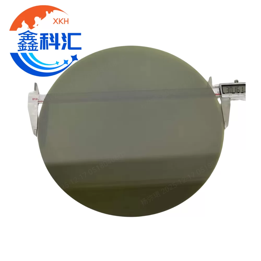
Silicon carbide (SiC) has emerged as a transformative material for power electronics, electric vehicles (EVs), renewable energy systems, and high-frequency applications. SiC offers significant advantages over traditional silicon, including higher breakdown voltage, faster switching speeds, and superior thermal conductivity. While SiC wafers have been commercially available for years in 4-inch, 6-inch, and more recently 8-inch formats, the industry’s attention is increasingly focused on 12-inch (300 mm) SiC wafers, which promise economies of scale and cost reduction. However, questions remain: Is the market technically and economically ready for mass production of 12-Zoll-SiC-Wafer?
Technological Innovations
Producing 12-inch SiC wafers presents considerable technical challenges due to the material’s inherent hardness and brittleness. Recent innovations have addressed several critical areas:
- Advanced Crystal Growth Methods
The majority of commercial SiC wafers are produced using Physical Vapor Transport (PVT), a high-temperature sublimation process. Scaling from 150 mm or 200 mm to 300 mm requires precise control of temperature gradients to reduce defects such as micropipes, stacking faults, and dislocations. New PVT furnace designs and process optimizations have improved yield, uniformity, and crystal quality in larger diameters. - Surface Preparation and Polishing
The hardness of SiC (Mohs ~9) makes wafer polishing extremely challenging. Innovations in chemical-mechanical polishing (CMP) and plasma-assisted techniques have enabled smoother surfaces and higher planarity for 12-inch wafers, critical for device fabrication and epitaxial layer deposition. - Epitaxial Layer Engineering
High-quality epitaxial layers are essential for power devices. Recent progress in SiC epitaxy on 12-inch substrates includes improved thickness uniformity and reduced defect density, allowing for consistent device performance across the wafer.
Market Readiness and Supply Chain Considerations
While technological hurdles are being overcome, mass production readiness depends on broader market factors:
- Manufacturing Infrastructure: Few fabs currently have the capability to handle 12-inch SiC wafers. Investments in new equipment, automation, and handling systems are required to prevent wafer breakage and contamination.
- Device Ecosystem: Power device manufacturers must adapt their fabrication lines to accommodate larger wafers. This includes redesigning masks, optimizing process flows, and adjusting equipment for higher throughput.
- Cost vs. Demand: 12-inch wafers reduce per-device cost by increasing yield and wafer area utilization. However, the upfront capital expenditure is significant. The market must reach a critical scale where adoption by EV and renewable energy sectors justifies the investment.
Opportunities Driving Adoption
- Electric Vehicle Market: EV powertrain systems increasingly demand high-efficiency inverters and chargers. SiC devices on 12-inch wafers offer better cost-performance ratios and are well-suited for mass-market EVs.
- Renewable Energy Applications: Large-scale solar inverters and energy storage systems benefit from high-voltage, high-efficiency SiC devices, which can be economically manufactured on larger wafers.
- High-Frequency and Aerospace Electronics: SiC devices can operate at elevated temperatures and frequencies, enabling applications in aerospace, defense, and industrial electronics that were previously constrained by silicon limitations.
Challenges and Future Outlook
Despite progress, several challenges remain:
- Defect Management: Even minor dislocations can impact device yield and reliability. Continuous improvements in crystal growth, wafer handling, and inspection are essential.
- Equipment Adaptation: Not all semiconductor fabs are equipped for 12-inch SiC processing, requiring retrofitting or new capital investment.
- Supply Chain Scaling: Raw SiC crystal growth and wafer slicing must scale to meet global demand without compromising quality.
Experts predict that mass adoption of 12-inch SiC wafers will likely follow the growth trajectory of 300 mm silicon wafers, but with a few years’ lag due to material and manufacturing complexities. Industry collaborations, co-investments, and standardization will accelerate readiness.
Schlussfolgerung
12-inch SiC wafers represent a significant technological and economic milestone for the semiconductor industry. While innovations in crystal growth, surface preparation, and epitaxial deposition have made high-quality large-diameter wafers feasible, full-scale mass production depends on ecosystem adaptation, cost reduction, and supply chain readiness. As EVs, renewable energy systems, and high-frequency electronics continue to expand, the demand for 12-inch SiC wafers will likely grow, positioning them as a cornerstone of next-generation power electronics.
FAQs
- Why are 12-inch SiC wafers important compared to smaller sizes?
Larger wafers increase chip yield per wafer and reduce per-device costs, enabling more economical mass production for EV and renewable energy applications. - What are the main technical challenges in producing 12-inch SiC wafers?
Key challenges include controlling crystal defects, polishing extremely hard surfaces, and ensuring epitaxial layer uniformity over a larger area. - Is the market ready to adopt 12-inch SiC wafers at scale?
While technology is progressing rapidly, widespread adoption depends on fab infrastructure, device ecosystem adaptation, and cost-benefit considerations.