
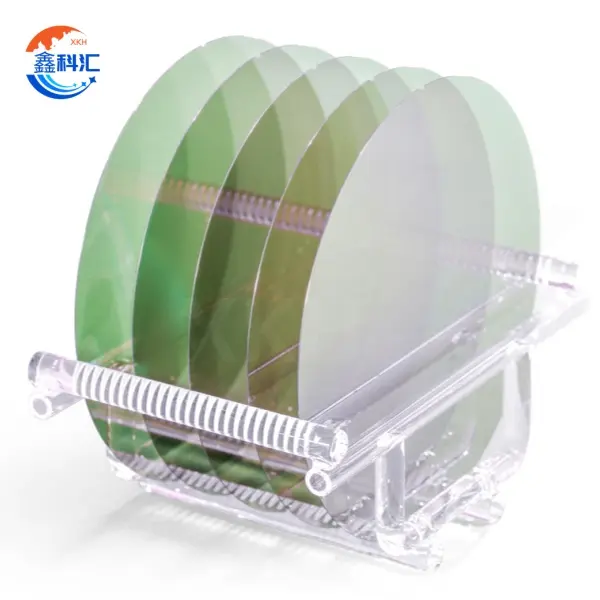
Silicon carbide (SiC) wafers have become a foundational material for high-power, high-frequency, and high-temperature electronics, particularly in electric vehicles, renewable energy systems, fast chargers, and industrial power converters. While much attention is often placed on SiC’s intrinsic material advantages—such as wide bandgap, high thermal conductivity, and high breakdown field—the surface quality of the SiC wafer plays an equally critical role in determining device performance, reliability, and lifetime.
This article explains how Oblea de SiC surface quality affects device lifetime, why surface defects matter, and how modern manufacturing techniques aim to control and improve surface integrity.
1. Why Surface Quality Matters in SiC Devices
In power semiconductor devices such as SiC MOSFETs, Schottky diodes, and epitaxial structures, the active device layers are built directly on or above the SiC substrate surface. Any imperfection on this surface can propagate through the epitaxial layer and ultimately impact electrical performance and long-term reliability.
Unlike silicon, SiC is much harder and more chemically inert, making it more difficult to polish and process. As a result, achieving a defect-free or ultra-smooth surface is both technically challenging and industrially significant.
The key reasons surface quality is critical include:
- Defects can create local electric field concentrations
- Surface roughness can degrade interface properties
- Subsurface damage can initiate cracks or reliability failures
- Surface irregularities can reduce epitaxial layer uniformity
All of these factors directly influence device lifetime.
2. Types of Surface Defects on SiC Wafers
Several categories of surface-related imperfections can affect SiC wafers:
2.1 Surface Roughness
Surface roughness refers to microscopic height variations on the wafer surface. If roughness is too high, it can:
- Reduce epitaxial layer uniformity
- Increase scattering of charge carriers
- Create localized stress points
This can lead to higher leakage currents and reduced device stability over time.
2.2 Scratches and Polishing Marks
Mechanical polishing is required to achieve mirror-like SiC surfaces, but improper polishing can leave scratches or micro-cracks. These defects may:
- Act as initiation sites for fracture
- Reduce mechanical strength
- Create weak points under thermal cycling
Devices operating at high temperatures are particularly sensitive to such imperfections.
2.3 Subsurface Damage
Even if the surface appears smooth, damage beneath the surface can exist due to grinding or cutting processes. This subsurface damage can:
- Weaken the wafer structurally
- Interact with electric fields in power devices
- Lead to premature device failure
Advanced chemical-mechanical polishing (CMP) is often used to minimize this issue.
3. How Surface Quality Affects Device Lifetime
3.1 Impact on Electrical Reliability
Surface defects can distort the local electric field distribution within a device. In high-voltage applications, this can cause:
- Increased risk of breakdown
- Localized heating
- Accelerated degradation
Over time, these effects shorten the operational lifetime of the device.
3.2 Impact on Thermal Stability
SiC devices often operate at temperatures above 150°C. Surface imperfections can trap heat or create thermal hotspots, which:
- Reduce heat dissipation efficiency
- Increase thermal stress
- Lead to material fatigue
Better surface quality enables more uniform heat flow and longer device life.
3.3 Impact on Epitaxial Layer Growth
Most SiC power devices rely on epitaxial layers grown on the substrate. If the underlying wafer surface is not sufficiently smooth or defect-free, the epitaxial layer may inherit these imperfections, leading to:
- Higher defect density in the active layer
- Lower yield in device fabrication
- Reduced long-term reliability
Thus, substrate surface quality is foundational to high-performance SiC electronics.
4. Industry Approaches to Improving Surface Quality
To ensure long device lifetime, manufacturers employ several techniques:
- Advanced CMP (Chemical Mechanical Polishing) to achieve ultra-smooth surfaces
- Defect inspection using AFM and optical microscopy
- Thermal annealing to relieve subsurface stress
- Laser or plasma surface treatment for defect reduction
These processes collectively aim to minimize both surface and subsurface imperfections.
5. Why Surface Quality is More Critical in SiC than Silicon
Compared to silicon, SiC devices operate at much higher electric fields and temperatures. This makes them more sensitive to surface imperfections. Even small defects that might be tolerable in silicon can be catastrophic in SiC power devices.
Therefore, strict control of surface quality is not optional—it is essential for reliable SiC-based electronics.
6. Conclusión
The surface quality of SiC wafers plays a decisive role in determining device lifetime, reliability, and performance. Surface roughness, scratches, and subsurface damage can all negatively impact electrical behavior, thermal stability, and mechanical integrity.
As SiC continues to replace silicon in high-power applications, ongoing advancements in wafer polishing, defect inspection, and surface treatment will be crucial in enabling longer-lasting, more reliable power electronics.
For engineers and device manufacturers, understanding and controlling SiC wafer surface quality is not just a materials challenge—it is a key factor in the future of energy-efficient electronics.