
Silicon carbide wafers are essential substrates for power electronics, RF devices, high-temperature sensors and other demanding semiconductor applications. However, producing a device-ready SiC wafer is considerably more difficult than processing a conventional silicon wafer.
SiC combines high hardness, brittleness and strong chemical stability. These properties make the material valuable in harsh operating environments, but they also make slicing, grinding and polishing slow and technically demanding. Conventional mechanical processing can introduce scratches, residual stress and subsurface damage that must be removed before epitaxial growth or device fabrication.
The complete SiC wafering process therefore requires careful control at every stage—from crystal orientation and boule slicing to chemical mechanical polishing and final inspection.
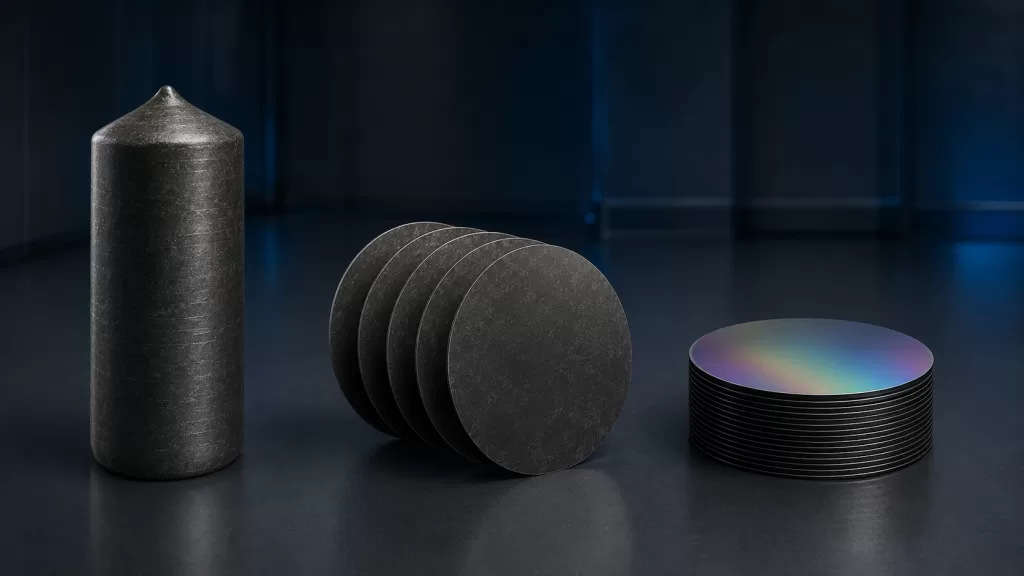
Overview of the SiC Wafer Processing Flow
| Processing stage | Main purpose | Important quality risks |
|---|---|---|
| Boule inspection | Confirm polytype, orientation and crystal quality | Incorrect orientation, excessive crystal defects |
| Cropping and shaping | Remove unusable ends and form the required diameter | Material loss, edge damage |
| Orientación de los cristales | Establish wafer surface orientation and off-axis angle | Orientation deviation |
| Boule slicing | Separate the boule into individual wafers | Kerf loss, saw marks, microcracks |
| Edge profiling | Form a controlled wafer edge | Edge chipping and fracture |
| Lapping or grinding | Improve thickness and flatness | Subsurface damage and residual stress |
| Damage removal | Remove mechanically affected layers | Insufficient material removal |
| Precision polishing | Reduce roughness and eliminate fine scratches | Polishing defects and nonuniformity |
| CMP finishing | Produce an epi-ready surface | Low removal rate, slurry residue |
| Limpieza | Remove particles, metals and organics | Contaminación superficial |
| Final inspection | Verify dimensions, surface and crystal quality | Undetected defects |
| Clean packaging | Protect the finished wafer during transport | Particles and mechanical damage |
1. Incoming SiC Boule Inspection
The process begins with a single-crystal SiC boule, usually produced through physical vapor transport, or PVT. Before mechanical processing begins, the boule must be evaluated to determine whether it satisfies the requirements of the intended wafer product.
Important inspection items include:
- SiC polytype, such as 4H-SiC or 6H-SiC
- Conductivity type, including N-type or semi-insulating material
- Orientación de los cristales
- Target off-axis angle
- Boule diameter and usable length
- Resistivity and doping uniformity
- Micropipes, inclusions and other crystal defects
- Internal stress and structural uniformity
For power device substrates, 4H-SiC is widely used because of its electrical properties. Depending on the application, wafers may be produced with an on-axis orientation or a controlled off-axis angle. A 4° off-axis orientation toward a defined crystallographic direction is commonly used for homoepitaxial growth, but the required orientation should always be confirmed before processing.
X-ray diffraction and other crystallographic measurement methods can be used to identify the crystal plane and establish the cutting direction.
2. Boule Cropping and Cylindrical Shaping
The top and bottom portions of an SiC boule may contain regions that are unsuitable for wafer production. These sections are removed during the cropping stage.
The remaining crystal is then shaped to achieve the required outer diameter. Cylindrical grinding can be used to improve diameter consistency and prepare the boule for subsequent slicing.
This stage may also include the formation of orientation features that will later be transferred to the individual wafers. Depending on the wafer diameter and specification, these features may include a notch or flat.
Because SiC is brittle, aggressive grinding conditions can generate edge cracks or deeper mechanical damage. Process parameters must balance material removal efficiency against crystal integrity.
3. Crystal Orientation and Cutting Alignment
Before slicing, the boule must be accurately aligned according to the required wafer orientation.
Important orientation parameters may include:
- Basal plane orientation
- Si-face or C-face designation
- On-axis or off-axis surface
- Off-axis angle
- Off-cut direction
- Notch orientation
The Si-face corresponds to the silicon-terminated surface, while the C-face is carbon-terminated. These two surfaces have different chemical and polishing behavior. For many power semiconductor applications, the Si-face is used as the front, epitaxy-ready surface.
Even a small orientation error can affect epitaxial step flow, surface morphology and subsequent device processing. Accurate alignment before slicing is therefore essential.
4. SiC Boule Slicing
After orientation, the boule is sliced into individual wafers. Fixed-abrasive diamond wire sawing is a commonly used method because diamond abrasives can process the extremely hard SiC crystal.
During wire sawing, a moving diamond-coated wire removes material and gradually separates wafers from the boule. The process must control:
- Wire speed
- Boule feed rate
- Wire tension
- Abrasive size
- Coolant or cutting fluid
- Contact length
- Cutting temperature
- Wire wear
- Wafer thickness allowance
Wire sawing is one of the most important yield-determining stages. Excessive cutting force or temperature can increase surface roughness, residual stress, wafer deformation and diamond-wire wear. Experimental research on monocrystalline 4H-SiC has also shown that sawing contact length and temperature influence the resulting wafer surface quality. ScienceDirect research on 4H-SiC diamond wire sawing
The as-sawn wafer normally contains:
- Parallel saw marks
- Surface grooves
- Microcracks
- Fichas de borde
- Thickness variation
- Daños subyacentes
- Residual mechanical stress
These conditions are expected at this stage, but sufficient processing allowance must remain so the damaged layer can be removed later.
Kerf loss is another major concern. Every cut consumes part of the expensive SiC boule, so wire diameter and cutting stability directly affect the number of usable wafers obtained from each crystal.
5. Wafer Edge Profiling
Freshly sliced SiC wafers have sharp, fragile edges. These edges can chip during handling or introduce cracks that propagate into the active wafer area.
Edge grinding is therefore used to produce a controlled bevel or rounded profile. A suitable edge geometry improves mechanical strength and reduces breakage during polishing, cleaning, epitaxy and device fabrication.
The finished edge should be inspected for:
- Chips
- Cracks
- Irregular bevel width
- Sharp transitions
- Edge contamination
- Dimensional deviation
Edge geometry must be matched to the wafer diameter, thickness, handling equipment and customer specification.
6. Lapping and Grinding
The as-sawn wafer is not yet sufficiently flat or smooth for semiconductor processing. Lapping or precision grinding is used to remove saw marks, improve thickness consistency and establish the basic wafer geometry.
Processing may be performed on one or both sides. Double-side grinding or lapping can help control total thickness variation and improve parallelism between the two surfaces.
Typical objectives include:
- Removing wire-saw marks
- Reducing wafer thickness
- Improving front-to-back parallelism
- Controlling TTV
- Reducing bow and warp
- Preparing the surface for fine polishing
Coarser abrasives provide higher removal rates but create deeper damage. Fine abrasives reduce the depth of the remaining damage layer but process the wafer more slowly. Manufacturers therefore normally use a staged approach, moving from coarse to fine abrasives.
Mechanical grinding does not only alter the visible surface. It can also create buried cracks, dislocations and residual stress below the surface. Research into wire-sawn single-crystal SiC has demonstrated that subsurface microcrack depth is an important factor in downstream processing.
7. Removing Subsurface Damage
A wafer may appear smooth after grinding while still containing a mechanically damaged layer beneath the surface. If this layer is not adequately removed, it can affect wafer strength, epitaxial growth and device yield.
Damage removal may involve a combination of:
- Fine grinding
- Mechanical polishing
- Chemical etching
- Chemical-assisted polishing
- Repeated surface inspection
The required removal depth depends on the slicing method, abrasive size and grinding conditions used earlier in the process.
Removing too little material leaves residual damage. Removing too much reduces boule utilization and may push the wafer below its target thickness. The process must therefore be based on controlled material-removal allowances rather than surface appearance alone.
8. Mechanical and Precision Polishing
After grinding, the wafer enters progressively finer polishing stages. The objective is to reduce surface roughness, remove scratches and prepare the wafer for final CMP.
Diamond abrasives may be used during intermediate polishing because of the hardness of SiC. However, purely mechanical polishing can continue to introduce fine scratches and subsurface damage.
The Si-face and C-face can behave differently during polishing. They may require different polishing conditions, pressures, slurry chemistries or processing times. Manufacturers must also determine whether the final product requires single-side polishing or double-side polishing.
Single-side polished wafers may be suitable for certain research, test and production applications. Double-side polished wafers are often selected when backside surface condition, optical transmission, flatness or advanced wafer handling is important.
9. Chemical Mechanical Polishing
Chemical mechanical polishing is usually the final surface-finishing stage for an epi-ready SiC wafer.
CMP combines chemical surface modification with gentle mechanical removal. In a typical mechanism, an oxidizing component modifies the chemically stable SiC surface, creating a softer reaction layer. Abrasive particles and the polishing pad then remove this modified material.
CMP is widely used to reduce roughness and remove residual subsurface damage from SiC wafers. However, its material-removal rate is relatively low because SiC is both hard and chemically inert.
- Slurry chemistry
- Oxidizer concentration
- Abrasive material and particle size
- Slurry pH
- Pad type and conditioning
- Downforce
- Wafer and platen rotation speeds
- Temperatura
- Polishing time
- Si-face or C-face processing
The finished surface must be smooth without introducing polishing scratches, pits, haze or localized nonuniformity.
Emerging methods—including plasma-assisted, electrochemical and photocatalytic polishing—attempt to increase material-removal efficiency by first converting the SiC surface into a softer layer. Research has demonstrated that controlled surface oxidation followed by soft-abrasive removal can reduce mechanical damage.
10. Post-Polishing Cleaning
CMP can leave slurry particles, organic residues, polishing-pad debris, ionic contamination and trace metals on the wafer.
Post-polishing cleaning must remove these contaminants without scratching the surface or changing its chemical condition. Depending on the process, cleaning may include:
- Megasonic or ultrasonic cleaning
- Surfactant-assisted cleaning
- Acid or alkaline cleaning
- Ozonated water
- DI water rinsing
- Spin rinsing and drying
- Filtered nitrogen drying
Cleaning chemistry must be compatible with the polished SiC surface and any applicable backside finish.
Handling is equally important. A fully polished wafer can be damaged by contaminated tweezers, carriers, cassettes or packaging materials.
11. Final SiC Wafer Inspection
A device-ready wafer must pass dimensional, surface, electrical and crystallographic inspection.
Dimensional inspection
Common dimensional parameters include:
- Diámetro
- Espesor
- Total thickness variation
- Bow
- Warp
- Edge profile
- Notch dimensions
- Notch orientation
- Exclusión de bordes
TTV describes thickness variation across the wafer. Bow indicates the central deviation of a free wafer from a reference plane, while warp represents the overall peak-to-valley deformation. These parameters affect wafer handling, chucking, lithography and epitaxial processing.
Surface inspection
The polished surface may be evaluated for:
- Rugosidad de la superficie
- Arañazos
- Pits
- Haze
- Stains
- Residual particles
- Fichas de borde
- Orange-peel texture
- Polishing marks
- Localized surface defects
Atomic force microscopy is commonly used for nanoscale roughness measurement, while optical inspection and interferometry can evaluate surface morphology and wafer shape.
Crystal and electrical inspection
Depending on the wafer grade and application, inspection may also include:
- Polytype confirmation
- Orientation measurement
- Off-axis angle
- Resistividad
- Carrier concentration
- Densidad de microtubos
- Dislocaciones del plano basal
- Dislocaciones de tornillos de rosca
- Threading edge dislocations
- Fallos de apilamiento
No single inspection method detects every defect type. Optical inspection, photoluminescence and X-ray topography provide complementary information and can be combined to improve defect identification.
What Makes a SiC Wafer Device-Ready?
“Device-ready” or “epi-ready” does not refer only to a shiny surface. It describes a wafer that meets the complete set of requirements needed for subsequent epitaxy or device fabrication.
A device-ready SiC wafer should generally provide:
- Correct polytype and conductivity type
- Controlled crystal orientation and off-axis angle
- Stable diameter and thickness
- Acceptable TTV, bow and warp
- Properly finished edges
- Low surface roughness
- Minimal scratches, pits and subsurface damage
- Controlled crystal-defect density
- Low particle and metal contamination
- Clean, semiconductor-compatible packaging
Exact acceptance limits depend on wafer diameter, device design, epitaxy process and customer specification. Surface roughness should therefore always be stated together with the measurement method, scan area and inspected wafer face.
Information Buyers Should Confirm
Before ordering processed SiC wafers, buyers should specify:
- Diámetro de la oblea
- 4H-SiC or 6H-SiC
- N-type or semi-insulating material
- Dopant and resistivity range
- On-axis or off-axis orientation
- Off-axis angle and direction
- Si-face or C-face
- Target thickness and tolerance
- TTV, bow and warp limits
- Single-side or double-side polishing
- Surface roughness requirement
- Prime, research, test or dummy grade
- Edge and notch requirements
- Required defect inspection
- Quantity and packaging method
Providing these parameters helps the supplier select an appropriate boule and establish sufficient slicing, grinding and polishing allowances.
Conclusión
Transforming a SiC boule into a device-ready wafer requires much more than simply cutting and polishing a hard crystal. Each processing stage affects the next.
Wire sawing determines kerf loss and initial subsurface damage. Grinding establishes thickness and flatness but can introduce residual stress. CMP creates the final low-roughness surface, while cleaning and inspection determine whether the wafer is suitable for epitaxy and semiconductor fabrication.
For buyers, understanding this processing flow makes it easier to evaluate wafer quality, compare specifications and communicate technical requirements with a SiC wafer supplier.
Frequently Asked Questions
Why is SiC more difficult to process than silicon?
SiC is harder, more brittle and more chemically inert than silicon. These characteristics reduce machining and polishing efficiency while increasing the risk of scratches, microcracks and subsurface damage.
What method is commonly used to slice an SiC boule?
Fixed-abrasive diamond wire sawing is widely used. Laser-assisted and laser-based slicing methods are also being developed to reduce kerf loss and mechanical damage.
Why is CMP necessary for SiC wafers?
Mechanical grinding and polishing can leave scratches and subsurface damage. CMP chemically modifies the SiC surface and gently removes the modified layer, producing a smoother surface suitable for epitaxy.
What is the difference between the Si-face and C-face?
The Si-face is silicon-terminated, while the C-face is carbon-terminated. They have different oxidation, polishing and epitaxial-growth behavior and may require different processing conditions.
What should be inspected on a finished SiC wafer?
Important items include thickness, TTV, bow, warp, surface roughness, scratches, particles, orientation, resistivity, edge quality and crystal defects.