
1. Johdanto
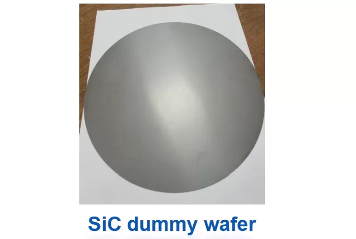
In semiconductor manufacturing, a dummy wafer (also known as a monitor wafer or blank wafer) is a non-device-bearing wafer used to support and stabilize process conditions. Among various materials, the Silicon Carbide (SiC) dummy wafer has gained increasing importance due to its outstanding thermal, mechanical, and chemical stability in extreme processing environments.
This article provides a scientific overview of SiC dummy wafers, covering their material properties, functional roles, applications, and future development trends.
2. What Is a Dummy Wafer?
A dummy wafer is a wafer that does not contain active devices but is used during semiconductor processing to:
- Fill empty slots in wafer carriers or boats
- Stabilize thermal distribution in process chambers
- Maintain uniform gas flow dynamics
- Protect equipment surfaces from direct exposure
- Improve process repeatability and consistency
Dummy wafers are widely used in processes such as CVD (Chemical Vapor Deposition), PVD (Physical Vapor Deposition), etching, and thermal annealing.
3. Why Silicon Carbide (SiC)?
Silicon Carbide is a wide bandgap material with a strong covalent crystal structure, giving it exceptional physical and chemical properties.
3.1 Key Material Comparison
| Kiinteistö | SiC Dummy Wafer | Pii (Si) | Quartz (SiO₂) |
|---|---|---|---|
| Lämmönjohtavuus | Very High (120–490 W/m·K) | Kohtalainen | Matala |
| High-Temperature Stability | >1200°C | ~600°C | ~1000°C |
| Kemiallinen kestävyys | Erinomainen | Kohtalainen | Hyvä |
| Mechanical Strength | Erittäin korkea | Medium | Brittle |
| Plasma Resistance | Erinomainen | Kohtalainen | Kohtalainen |
SiC clearly outperforms conventional materials in harsh semiconductor processing environments.
4. Functional Roles in Semiconductor Processing
4.1 Thermal Field Stabilization
In high-temperature processes such as annealing and epitaxial growth, SiC dummy wafers help:
- Improve temperature uniformity across wafer batches
- Reduce thermal gradients
- Minimize wafer warping and stress defects
4.2 Gas Flow and Plasma Uniformity
During CVD and plasma etching processes:
- Dummy wafers fill empty positions in wafer carriers
- Ensure stable gas distribution in the chamber
- Reduce turbulence and process variation
Because SiC is chemically inert, it does not interfere with process chemistry.
4.3 Equipment Protection
In plasma-rich environments such as dry etching:
5. Types of SiC Dummy Wafers
5.1 Polycrystalline SiC (Poly-SiC)
- Lower production cost
- Suitable for general industrial use
- Often used with surface polishing or coatings
5.2 Single-Crystal SiC
- High purity and structural uniformity
- Used in advanced semiconductor processes
- Superior thermal and mechanical performance
5.3 Coated SiC Wafers
- Silicon or quartz substrate with SiC coating
- Balanced cost-performance solution
- Widely used in mid-range applications
6. Application Areas
6.1 Semiconductor Manufacturing Equipment
SiC dummy wafers are commonly used in:
- CVD systems
- PVD systems
- Dry etching chambers
- Rapid thermal processing (RTP)
6.2 Power Semiconductor Production
In Power Electronics manufacturing, SiC dummy wafers improve process stability for high-voltage and high-efficiency devices.
6.3 Optoelectronics and LED Industry
SiC dummy wafers are also used in:
- Sapphire-based epitaxy processes
- LED wafer growth
- Thermal stabilization during deposition
7. Technical Challenges
Despite its advantages, SiC dummy wafer technology faces several challenges:
- High manufacturing cost, especially for single-crystal SiC
- Difficult machining, due to extreme hardness
- Strict surface flatness requirements
- Complex cleaning and reuse processes
These factors limit large-scale adoption in cost-sensitive applications.
8. Future Development Trends
8.1 Higher Purity and Lower Defect Density
Driven by advanced semiconductor nodes requiring extreme process stability.
8.2 Composite Wafer Structures
Hybrid designs such as SiC-on-Si or SiC-coated ceramics to reduce cost.
8.3 Process-Specific Customization
Optimized dummy wafer placement based on simulation of thermal and gas flow fields.
8.4 Increased Use in Advanced Packaging
Growing demand from 3D packaging and heterogeneous integration technologies.
9. Päätelmät
The Silicon Carbide dummy wafer plays a crucial yet often invisible role in modern semiconductor manufacturing. While it does not participate in device fabrication, it significantly enhances process stability, thermal uniformity, and equipment durability.
As semiconductor processes continue to evolve toward higher temperatures, greater precision, and more complex architectures, SiC dummy wafers are expected to become increasingly important in next-generation manufacturing ecosystems.