
As integrated photonics continues to move toward higher bandwidth, lower power consumption, and smaller device footprints, material platforms are becoming increasingly important. Traditional optical materials such as bulk lithium niobate, silicon photonics, and silicon nitride each provide specific advantages, but they also introduce limitations in electro-optic efficiency, optical confinement, or integration density.
Thin-Film Lithium Niobate (TFLN) has emerged as one of the most promising material platforms for next-generation photonic devices.
By transferring a sub-micron lithium niobate layer onto an insulating substrate, TFLN combines the outstanding electro-optic properties of lithium niobate with the manufacturing advantages of modern semiconductor processing.
This technology is now driving innovation across optical communication, quantum photonics, microwave photonics, and nonlinear optical systems.
What Is Thin-Film Lithium Niobate (TFLN)?
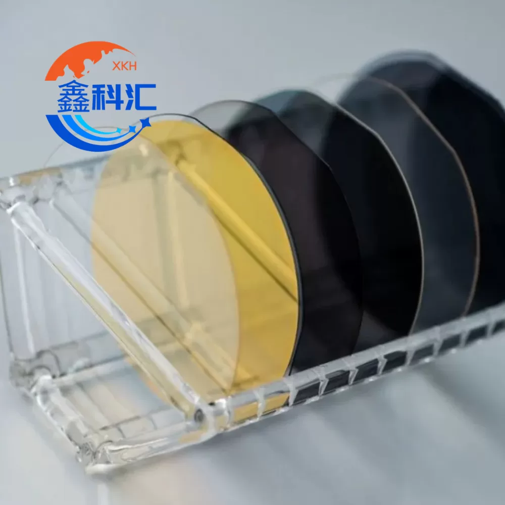
Thin-Film Lithium Niobate (TFLN) refers to a very thin single-crystal lithium niobate (LiNbO₃) layer, typically ranging from several hundred nanometers to around one micrometer in thickness.
Unlike conventional bulk lithium niobate crystals, TFLN is fabricated as a thin device layer integrated onto an insulating platform.
The resulting structure is commonly implemented as:
| Layer | Materiaali |
|---|---|
| Device Layer | Thin-film LiNbO₃ |
| Insulating Layer | SiO₂ |
| Handle Substrate | Silicon / Quartz / Sapphire |
This architecture is widely known as a Lithium Niobate on Insulator (LNOI) platform.
The thin-film structure enables stronger optical confinement and substantially improves electro-optic interaction efficiency.
Why Bulk Lithium Niobate Reached Its Limits
Lithium niobate has long been a key optical material because of its:
- Strong electro-optic effect
- Excellent nonlinear optical characteristics
- Wide optical transparency window
- Piezoelectric behavior
- High optical damage threshold
For decades, bulk lithium niobate modulators dominated optical communication systems.
However, conventional bulk devices also introduced significant challenges:
| Limitation | Bulk LiNbO₃ |
|---|---|
| Device footprint | Large |
| Integration density | Rajoitettu |
| Modulation voltage | Korkea |
| Optical confinement | Weak |
| CMOS integration | Difficult |
As communication systems moved toward 400G, 800G, and future 1.6T architectures, these limitations became increasingly restrictive.
Researchers began seeking methods to preserve lithium niobate performance while enabling wafer-scale photonic integration.
Core Principle of TFLN Technology
The key innovation behind TFLN lies in converting lithium niobate from a bulk crystal into a semiconductor-compatible thin-film platform.
Reducing the film thickness dramatically increases optical mode confinement.
As optical energy becomes concentrated inside sub-micron waveguides:
- Electro-optic interaction becomes stronger
- Device dimensions become smaller
- Modulation efficiency improves
- Driving voltage decreases
- Power consumption is reduced
In practical photonic devices, stronger confinement allows engineers to achieve much higher performance with significantly smaller structures.
This principle has transformed lithium niobate from a discrete optical material into a scalable integrated photonics platform.
Fabrication Process of TFLN
The production of Thin-Film Lithium Niobate typically involves advanced wafer engineering techniques.
The fabrication flow generally includes:
Ion Implantation
High-energy ions are implanted into bulk lithium niobate crystals to define a controlled cleavage layer.
Wafer Bonding
The implanted crystal is bonded to a silicon dioxide coated substrate.
Layer Transfer
Thermal treatment separates a thin crystalline lithium niobate layer from the original crystal.
Chemical Mechanical Polishing
CMP processing creates extremely smooth surfaces suitable for low-loss waveguides.
Wafer Inspection
Surface roughness, defect density, and optical properties are measured.
Advantages of TFLN Over Traditional Platforms
Compared with bulk lithium niobate and many competing photonic platforms, TFLN offers several major advantages.
| Kiinteistö | Bulk LiNbO₃ | TFLN Platform |
|---|---|---|
| Optical Loss | Higher | Ultra-low |
| Device Size | Large | Compact |
| Integration Density | Rajoitettu | Korkea |
| Electro-optic Efficiency | Kohtalainen | Korkea |
| Modulation Voltage | Higher | Lower |
| Silicon Integration | Difficult | Compatible |
Typical waveguide propagation loss can be lower than:
< 0.05 dB/cm
while maintaining strong electro-optic performance.
Key Applications of Thin-Film Lithium Niobate
Optical Communication
High-speed electro-optic modulators based on TFLN are rapidly replacing conventional technologies.
Sovelluksia ovat mm:
- Coherent optical transceivers
- Data center optical interconnects
- 400G and 800G communication systems
- Future 1.6T optical networks
Quantum Photonics
Quantum systems require precise manipulation of photons.
TFLN supports:
- Entangled photon generation
- Quantum key distribution
- Integrated quantum circuits
- Quantum optical processing
Microwave Photonics
Combining optical and microwave functions enables:
- RF photonic filtering
- Beamforming systems
- Optical phased arrays
- Millimeter-wave processing
Nonlinear Optics
Lithium niobate possesses strong second-order nonlinear coefficients.
Sovelluksia ovat mm:
- Frequency conversion
- Frequency comb generation
- Optical parametric oscillation
- Harmonic generation
Optical Sensing
Integrated TFLN devices are increasingly used in:
- Biochemical sensors
- Environmental monitoring
- High-sensitivity resonators
- Precision optical measurements
Future Trends of TFLN Technology
TFLN is evolving from a research material toward high-volume manufacturing.
Current industry development focuses on:
- Larger wafer diameters (6–8 inch and beyond)
- Lower propagation loss targets
- Hybrid integration with silicon photonics
- Improved modulation efficiency
- AI and data center photonic applications
Future communication systems will demand faster, smaller, and more energy-efficient optical devices.
TFLN is positioned as a major candidate platform for meeting these requirements.
Päätelmä
Thin-Film Lithium Niobate represents a major shift in photonic engineering.
By combining the superior electro-optic properties of lithium niobate with semiconductor-compatible fabrication processes, TFLN enables a new generation of compact and high-performance photonic devices.
As integrated photonics continues to expand into communication, sensing, and quantum technologies, TFLN is expected to become one of the most influential material platforms of the coming decade.
FAQ
What is Thin-Film Lithium Niobate used for?
TFLN is widely used in optical communication, quantum photonics, microwave photonics, and integrated optical devices.
What is the difference between TFLN and LNOI?
TFLN refers to the lithium niobate thin-film layer itself, while LNOI refers to the complete wafer platform including the thin film, oxide layer, and substrate.
Why is TFLN better than bulk lithium niobate?
TFLN provides stronger optical confinement, smaller device size, lower power consumption, and better integration capability.