
Semiconductor wafers must be protected from particles, mechanical damage, electrostatic contamination and handling errors throughout manufacturing and transportation.
However, not every wafer carrier is designed for the same purpose.
Three terms frequently encountered in semiconductor manufacturing are FOUP, FOSB and wafer cassette. Although all three are used to hold and protect wafers, their structures, cleanliness requirements, automation compatibility and intended applications are significantly different.
For semiconductor fabs, equipment manufacturers, wafer suppliers and advanced packaging facilities, selecting the correct wafer carrier is important not only for wafer protection but also for maintaining process stability and compatibility with automated material handling systems.
This guide explains the differences between FOUPs, FOSBs and wafer cassettes, with particular attention to 300mm wafer handling, transportation, cleanroom use and semiconductor automation.
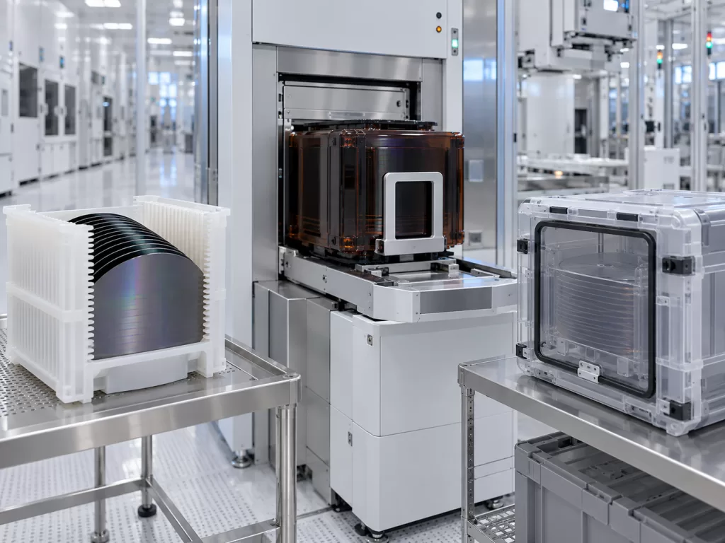
What Is a FOUP?
FOUP stands for Front Opening Unified Pod.
It is an enclosed wafer carrier primarily associated with 300mm semiconductor wafer manufacturing and highly automated semiconductor fabs.
Unlike traditional open wafer cassettes, a FOUP completely encloses the wafers and uses a standardized front-opening door. Semiconductor processing equipment can open the FOUP automatically without requiring an operator to manually remove the wafers.
This design makes the FOUP an important component of modern automated fabs.
Typical applications include:
- 300mm silicon wafer manufacturing
- Logic semiconductor fabs
- Memory semiconductor production
- Advanced semiconductor process lines
- Automated wafer transport
- Lithography
- Deposition
- Etching
- Ion implantation
- CMP
- Cleaning
- Metrology
A standard 300mm FOUP commonly carries multiple wafers in vertically separated slots, often up to 25 wafers depending on the configuration.
The carrier interfaces with equipment load ports, wafer-handling robots and automated material handling systems.
Why FOUPs Are Important in 300mm Semiconductor Fabs
As semiconductor geometries become smaller, contamination control becomes increasingly important.
A particle that might have been relatively insignificant in an older semiconductor process can cause defects in advanced semiconductor devices.
FOUPs help create a controlled mini-environment around the wafers.
Instead of exposing wafers to the entire cleanroom whenever they are transported, wafers remain inside the enclosed carrier.
This provides several advantages.
Improved Particle Protection
The enclosed structure helps reduce direct exposure to airborne particles during transportation between semiconductor processing tools.
Reduced Manual Handling
FOUPs are designed for robotic loading and unloading, significantly reducing the need for operators to touch or manually transfer wafer carriers.
AMHS Compatibility
FOUPs can be integrated with an Automated Material Handling System, commonly abbreviated as AMHS.
Depending on the fab architecture, FOUPs may be transported using systems such as:
- overhead transport
- stockers
- automated storage systems
- robotic transfer systems
- automated load ports
This makes FOUP technology particularly important in high-volume 300mm wafer fabs.
Better Process Traceability
FOUPs may also incorporate identification technologies that allow manufacturing systems to track wafer lots, carrier locations and process status.
This is important in semiconductor manufacturing environments where thousands of wafer movements may occur every day.
What Is a FOSB?
FOSB stands for Front Opening Shipping Box.
The external appearance of a FOSB can sometimes resemble a FOUP, which is why the two are frequently confused.
However, their primary functions are different.
A FOUP is designed mainly for wafer movement inside semiconductor manufacturing environments, while a FOSB is primarily designed for:
wafer shipping, transportation and storage.
FOSBs are commonly used by silicon wafer manufacturers, substrate suppliers and semiconductor material companies when transporting wafers to customers.
Typical applications include shipping:
- 300mm silicon wafers
- epitaxial wafers
- SOI wafers
- monitor wafers
- test wafers
- reclaim wafers
- some compound semiconductor substrates
The primary engineering priorities of a FOSB therefore include mechanical wafer protection, secure transportation and contamination control during logistics.
FOUP vs FOSB: What Is the Main Difference?
The simplest distinction is:
FOUP = semiconductor fab automation
FOSB = wafer transportation and shipping
Although both can hold 300mm wafers and use front-opening designs, they are optimized for different stages of the semiconductor supply chain.
| Feature | FOUP | FOSB |
|---|---|---|
| Primary purpose | Fab wafer handling | Shipping and transportation |
| Typical environment | Semiconductor cleanroom | Logistics, warehouse and cleanroom receiving |
| Automation requirement | High | Usually lower |
| Equipment load-port compatibility | Important | Not always required |
| AMHS integration | Common | Generally not the primary purpose |
| Wafer protection | High | Very high during transportation |
| Particle control | Critical | Critical |
| Mechanical shipping protection | Secondary | Major design requirement |
| Typical wafer size | Mainly 300mm | Commonly 300mm |
| Typical user | Semiconductor fab | Wafer manufacturer or substrate supplier |
Because FOUPs and FOSBs serve different functions, they should not automatically be considered interchangeable.
A carrier that works well for international wafer transportation may not meet the automation or interface requirements of a semiconductor production line.
Similarly, using a production FOUP purely as a shipping container may not be economically or operationally appropriate.
What Is a Wafer Cassette?
A wafer cassette is a more general type of wafer carrier used to hold multiple semiconductor wafers in individual slots.
Unlike a FOUP, many wafer cassettes have an open or partially open structure.
They are widely used throughout semiconductor manufacturing, laboratories, wafer processing lines and substrate handling operations.
Wafer cassettes are available for different wafer diameters, including:
- 2-inch wafers
- 3-inch wafers
- 4-inch wafers
- 5-inch wafers
- 6-inch / 150mm wafers
- 8-inch / 200mm wafers
- specialized wafer formats
They may also be manufactured for 300mm wafer applications, although fully automated advanced 300mm fabs generally rely heavily on enclosed carrier systems such as FOUPs.
Wafer cassettes can be used for:
- wafer cleaning
- wet processing
- wafer storage
- wafer inspection
- laboratory handling
- wafer transfer
- thermal processes
- temporary wafer storage
- research and development
The required cassette design depends heavily on the process environment.
FOUP vs Wafer Cassette
The biggest difference between a FOUP and a conventional wafer cassette is the degree of environmental isolation.
A typical wafer cassette exposes at least part of the wafer surfaces to the surrounding environment.
A FOUP encloses the wafers within a protective housing.
This distinction becomes increasingly important as wafer size increases and semiconductor process requirements become more stringent.
Wafer Cassette Advantages
Traditional wafer cassettes can offer:
- simpler construction
- lower cost
- easy visual inspection
- convenient manual handling
- suitability for wet processing
- compatibility with many laboratory systems
- flexibility for smaller wafer diameters
They remain widely used in semiconductor manufacturing.
FOUP Advantages
FOUPs provide advantages where contamination control and automation are critical:
- enclosed wafer environment
- compatibility with automated load ports
- reduced human contact
- automated lot transportation
- improved contamination control
- better integration with modern 300mm fabs
The correct choice therefore depends on the process rather than simply the wafer diameter.
FOUP vs FOSB vs Wafer Cassette at Different Manufacturing Stages
A single wafer may encounter multiple carrier types before becoming a finished semiconductor device.
Consider a typical 300mm silicon wafer supply chain.
Stage 1: Wafer Manufacturing
A silicon wafer manufacturer produces and inspects polished wafers.
After final cleaning and inspection, wafers must be packaged for delivery.
A FOSB may be used because the primary objective is safe transportation from the wafer supplier to the semiconductor fab.
Stage 2: Incoming Wafer Receiving
The semiconductor fab receives the wafers.
Incoming inspection may include:
- package inspection
- particle inspection
- wafer identification
- dimensional measurement
- surface inspection
The wafers may then be transferred into the carrier system used by the fab.
Stage 3: Semiconductor Processing
During device manufacturing, wafers travel repeatedly between process tools.
For advanced 300mm fabs, this is where the FOUP becomes particularly important.
FOUPs transport wafer lots between processes such as:
cleaning → oxidation → deposition → lithography → etching → implantation → CMP → metrology.
The carrier becomes part of the automated semiconductor manufacturing infrastructure.
Stage 4: Specialized Processing
Certain manufacturing operations may still use dedicated wafer cassettes, process carriers or custom holders.
For example, wet benches and specialized cleaning equipment may require carriers made from chemically resistant materials.
Therefore, semiconductor factories frequently use multiple types of wafer handling products rather than relying on only one carrier design.
Why Cleanliness Matters for Wafer Carriers
Carrier cleanliness can directly affect semiconductor yield.
Possible contamination sources include:
- particles
- organic residues
- metallic contamination
- outgassing
- electrostatic attraction
- wear particles
- residues from previous processes
The cleanliness requirement becomes particularly demanding for carriers used with advanced semiconductor processes.
Carrier materials, manufacturing processes and cleaning procedures must therefore be carefully controlled.
Important considerations can include:
Low Particle Generation
Carrier surfaces should minimize abrasion and particle shedding during wafer insertion, removal and transportation.
Chemical Compatibility
Materials must tolerate the cleaning chemicals and environmental conditions used in the target application.
Low Outgassing
Organic contaminants released from polymers may be undesirable in sensitive semiconductor environments.
Dimensional Stability
Accurate wafer slot positioning is important for robotic wafer handling.
If slot geometry changes or the carrier deforms, wafer-handling robots may fail to locate wafers correctly.
Material Selection for FOUPs, FOSBs and Wafer Cassettes
High-performance polymers are commonly used for semiconductor wafer carriers.
Depending on the application, important material characteristics may include:
- dimensional stability
- chemical resistance
- low particle generation
- mechanical strength
- impact resistance
- controlled electrical properties
- low contamination
- cleanroom compatibility
Different carrier components may use different polymer formulations.
A FOSB may place greater emphasis on transportation impact resistance and secure wafer retention.
A FOUP must additionally satisfy demanding dimensional and automation interface requirements.
Wet-process wafer cassettes may require strong resistance to acids, bases and process chemicals.
Material selection should therefore always be based on the actual semiconductor process environment.
300mm Automation and FOUP Load-Port Compatibility
One of the most important differences between a FOUP and a general wafer container is its interaction with semiconductor equipment.
In automated fabs, a FOUP may arrive at the load port without direct operator handling.
The equipment must accurately recognize and position the carrier before opening the front door and transferring wafers.
This requires precise control of:
- carrier dimensions
- door position
- wafer slot location
- mechanical interfaces
- carrier placement
- wafer spacing
Small dimensional deviations can create significant problems in automated wafer handling.
For this reason, semiconductor equipment manufacturers and wafer carrier suppliers must carefully manage tolerances and interface compatibility.
Can a FOSB Be Used as a FOUP?
Generally, users should not assume that a FOSB can directly replace a FOUP.
Although both may use a front-opening structure, their design priorities and equipment interfaces are different.
Before using any wafer carrier in automated semiconductor equipment, engineers should confirm:
- load-port compatibility
- mechanical interface dimensions
- wafer slot geometry
- automation requirements
- carrier identification requirements
- cleanliness specification
- equipment manufacturer’s recommendations
Using an incompatible carrier can cause wafer-handling errors or equipment interruptions.
Can a FOUP Be Used for Shipping?
A FOUP physically protects wafers and may be transported under controlled conditions, but this does not mean it is automatically the best shipping solution.
Commercial wafer transportation introduces different requirements, including:
- vibration
- shock
- logistics handling
- external packaging
- long transportation periods
- warehouse storage
- international shipment
FOSBs are specifically designed around the requirements of wafer transportation.
Therefore, wafer suppliers generally select the carrier according to the transportation and customer receiving requirements rather than assuming that every enclosed wafer carrier serves the same purpose.
How to Select the Right Wafer Carrier
When selecting between a FOUP, FOSB and wafer cassette, engineers should consider at least seven factors.
1. Wafer Diameter
Determine whether the carrier is required for 100mm, 150mm, 200mm, 300mm or another wafer size.
2. Manufacturing Stage
Is the carrier used for:
- shipping
- cleanroom transportation
- process equipment
- laboratory handling
- wet processing
- storage?
This often determines the carrier category immediately.
3. Automation Level
For highly automated semiconductor fabs, compatibility with robotic equipment and material-handling systems is critical.
4. Cleanliness Requirements
Advanced semiconductor manufacturing generally requires stricter particle and contamination control than ordinary laboratory storage.
5. Process Chemistry
Wet-process carriers must tolerate the chemicals used in cleaning and etching processes.
6. Mechanical Protection
Shipping containers require greater consideration of shock, vibration and wafer movement during transportation.
7. Equipment Interface
For automated equipment, mechanical dimensions and wafer slot positions must match the tool requirements.
FOUP, FOSB and Wafer Cassette Selection Summary
Choosing the right wafer carrier depends primarily on where and how the wafers will be handled.
A simple way to understand the three categories is:
FOUP
Best suited for highly automated 300mm semiconductor fabs where wafers must move between process equipment while remaining in a controlled mini-environment.
FOSB
Best suited for transporting and shipping semiconductor wafers between wafer manufacturers, distributors and semiconductor fabs.
Wafer Cassette
Best suited for flexible wafer handling, laboratory work, wet processes and many 100mm, 150mm and 200mm semiconductor manufacturing applications.
As semiconductor manufacturing moves toward larger wafer diameters, greater automation and tighter contamination control, wafer carriers are becoming increasingly important components of the overall manufacturing system.
They are no longer simply plastic boxes used to hold wafers.
In advanced semiconductor production, the wafer carrier forms part of the contamination-control strategy, material-handling architecture and equipment automation system.
Understanding the differences between FOUPs, FOSBs and wafer cassettes helps semiconductor manufacturers select the correct solution for wafer shipping, storage, processing and automated production.