
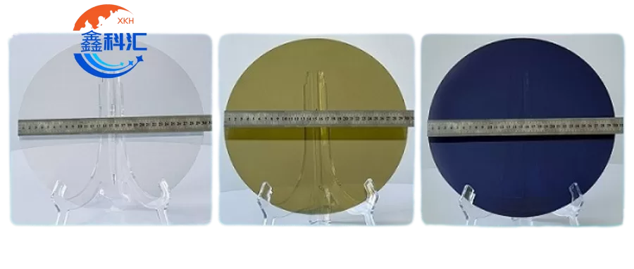
SiC wafers have become the foundation of next-generation high-power and high-voltage devices due to their wide bandgap, high thermal conductivity, and superior breakdown strength. While laboratory-level performance metrics are well documented, long-term reliability under real operating conditions remains a primary concern for power electronics engineers. This article reviews field data, failure statistics, and practical observations from high-power applications to clarify how Plaque de SiC quality influences long-term device reliability—and where the actual risks still lie.
1. Introduction: Why Long-Term Reliability Matters More Than Peak Performance
In high-power devices such as traction inverters, industrial motor drives, and power grids, reliability is often more critical than absolute efficiency.
A marginal efficiency gain becomes irrelevant if early-life failures, parametric drift, or catastrophic breakdown occurs after extended operation.
Unlike silicon-based devices, SiC devices typically operate at:
- Températures de jonction plus élevées
- Higher electric fields
- Higher switching frequencies
These conditions amplify latent defects within the wafer and make long-term field performance strongly dependent on substrate quality rather than device design alone.
2. Field Data vs. Laboratory Data: A Critical Distinction
2.1 Laboratory Qualification Is Necessary—but Insufficient
Standard reliability tests (HTRB, HTGB, power cycling, thermal cycling) are designed to accelerate known failure mechanisms. However, field data reveals failure modes that do not always manifest during qualification testing, especially those related to:
- Low-density crystal defects
- Wafer-scale non-uniformity
- Edge-related stress accumulation
2.2 What Field Data Consistently Shows
Across multiple industrial deployments, long-term field observations indicate:
| Observation | Field Trend |
|---|---|
| Early-life failures | Strongly correlated with wafer defect density |
| Mid-life degradation | Often linked to thermal stress and current crowding |
| Late-life failures | Dominated by electric field concentration near defects |
This confirms that wafer-level imperfections, even at very low density, can dominate lifetime reliability in high-power environments.
3. Dominant Wafer-Related Reliability Factors
3.1 Crystal Defects: Still the Primary Risk
Although micropipe density has been dramatically reduced in modern SiC substrates, other crystal imperfections remain critical, including:
- Dislocations du plan basal (BPD)
- Threading screw dislocations (TSDs)
- Local lattice distortion zones
Field data shows that devices fabricated on wafers with similar average defect density can still exhibit significantly different lifetimes, depending on defect clustering and spatial distribution.
3.2 Thermal Stress Accumulation Over Time
SiC’s high thermal conductivity is often seen as a reliability advantage. Field data suggests a more nuanced reality:
- Rapid thermal cycling introduces localized mechanical stress
- Stress concentrates near:
- Epitaxial/substrate interfaces
- Wafer edges
- Regions with thickness non-uniformity
Over long operating periods, this stress can:
- Accelerate defect propagation
- Induce micro-cracking
- Degrade metallization interfaces
3.3 Electric Field Enhancement at Defect Sites
High breakdown field strength is one of SiC’s greatest strengths—but also a reliability challenge.
Field measurements indicate that:
- Localized defects can act as electric field amplifiers
- Breakdown often initiates away from the designed active region
- Long-term degradation may occur without immediate catastrophic failure
This explains why some devices pass initial high-voltage tests but fail after prolonged operation.
4. Wafer Diameter and Thickness: Reliability Trade-Offs
As the industry transitions to larger-diameter SiC wafers, field data highlights several reliability considerations:
| Paramètres | Reliability Impact |
|---|---|
| Larger diameter | Higher risk of radial non-uniformity |
| Plaquettes plus minces | Increased mechanical stress sensitivity |
| Thickness variation | Uneven thermal expansion under load |
Field experience shows that mechanical robustness often matters more than theoretical performance margins in long-life applications.
5. What Field Failures Reveal About Manufacturing Priorities
5.1 Yield Optimization vs. Reliability Optimization
Field data consistently suggests:
- Maximizing wafer yield does not always maximize long-term reliability
- Aggressive thinning or polishing can introduce latent damage
- Cosmetic surface quality does not guarantee internal crystal integrity
5.2 Reliability Is Determined Early in the Supply Chain
Once device fabrication begins, most wafer-induced reliability risks are already locked in.
Later process optimization can mitigate—but not eliminate—substrate-originated weaknesses.
6. Practical Engineering Implications
Based on long-term field observations, several practical conclusions emerge:
- Lower defect density alone is not sufficient; defect distribution matters
- Conservative wafer thickness improves lifetime stability
- Edge quality and stress management deserve more attention than often assumed
- Wafer qualification should include application-specific stress profiles
For high-power systems designed for 10–20 years of service life, wafer selection is a reliability decision, not a procurement decision.
7. Conclusion: What Field Data Ultimately Tells Us
Field data confirms that SiC wafers can deliver exceptional long-term reliability—but only when substrate quality, mechanical robustness, and defect control are prioritized over short-term yield and cost optimization.
In high-power devices, the wafer is not just a starting material; it is a long-term reliability determinant.
Understanding this distinction is essential for engineers seeking to move from laboratory success to durable field performance.