
1. Introduction
Silicon carbide (SiC) has become a cornerstone material in power electronics, RF devices, and harsh-environment applications due to its wide bandgap, high thermal conductivity, and exceptional breakdown field. However, unlike silicon, Plaque de SiC selection is highly non-trivial. Subtle differences in polytype, doping, and defect density can directly determine device performance, yield, and long-term reliability.
This guide provides a deep, engineering-level overview of key SiC wafer specifications and offers practical selection strategies for buyers and process engineers.
2. Polytypes: 4H-SiC vs 6H-SiC vs 3C-SiC
2.1 What is a Polytype?
SiC exists in multiple polytypes, which are different stacking sequences of Si–C bilayers. These variations result in distinct electronic properties, even though the chemical composition is identical.
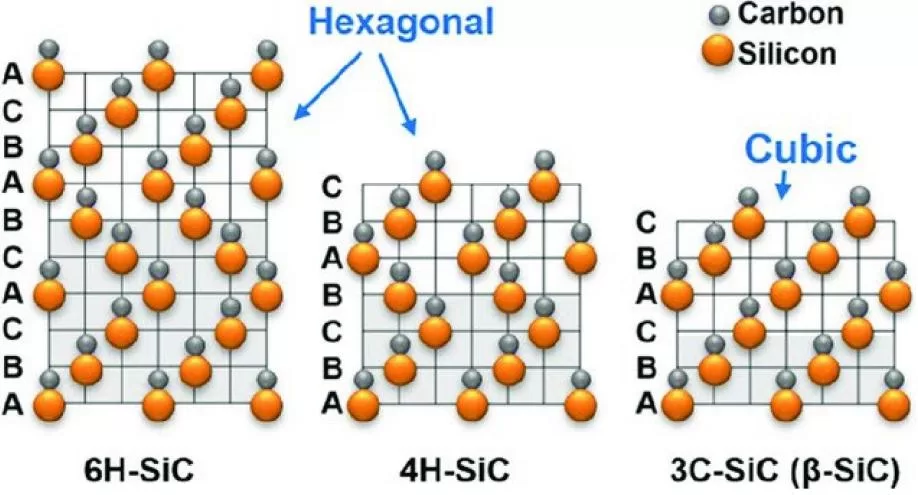
2.2 Key Polytypes Comparison
| Propriété | 4H-SiC | 6H-SiC | 3C-SiC |
|---|---|---|---|
| Crystal structure | Hexagonal | Hexagonal | Cubic |
| Bandgap (eV) | ~3.26 | ~3.02 | ~2.36 |
| Electron mobility | Haut | Modéré | Haut |
| Commercial maturity | ★★★★★ | ★★ | ★ |
| Utilisation typique | Power devices | RF (legacy) | Research / niche |
2.3 Selection Insight
- 4H-SiC → Industry standard for MOSFETs, Schottky diodes
- 6H-SiC → Largely phased out, limited niche usage
- 3C-SiC → Still under development, mainly on Si substrates
✔ Conclusion :
👉 In >90% of commercial cases, 4H-SiC is the correct choice
3. Doping: N-type, Semi-insulating, and Resistivity Control
3.1 Doping Types
| Type | Dopant | Résistivité | Application |
|---|---|---|---|
| N-type | Azote (N) | Low (0.015–0.03 Ω·cm) | Power devices |
| Semi-insulating (SI) | Vanadium (V) | Very high (>10⁵ Ω·cm) | RF / microwave |
| P-type | Aluminium (Al) | Modéré | Rare (substrate level) |
3.2 Engineering Implications
- N-type substrates
→ Enable vertical conduction
→ Used in SiC MOSFETs, diodes - Semi-insulating substrates
→ Suppress parasitic capacitance
→ Critical for GaN-on-SiC RF devices
3.3 Key Parameters to Specify
- Resistivity range (e.g., 0.02–0.025 Ω·cm)
- Dopant uniformity
- Carrier concentration
✔ Buyer Tip:
👉 Always request radial resistivity uniformity maps
4. Micropipes and Defects: The Yield Killer
4.1 What are Micropipes?
Micropipes are hollow-core screw dislocations that propagate along the crystal growth direction. They are among the most detrimental defects in SiC wafers.
4.2 Why They Matter
- Cause device breakdown failure
- Reduce yield dramatically
- Act as leakage paths
4.3 Defect Metrics
| Paramètres | Typical Spec |
|---|---|
| Micropipe density (MPD) | < 1 cm⁻² (modern wafers) |
| Threading dislocation density (TSD) | 10³–10⁵ cm⁻² |
| Basal plane dislocations (BPD) | Critical for reliability |
4.4 Industry Trend
- Early SiC: MPD > 100 cm⁻²
- Modern SiC: Near-zero micropipe wafers
✔ Conclusion :
👉 Micropipes are no longer the main issue
👉 BPD and TSD now dominate reliability concerns
5. Surface and Structural Specifications
5.1 Wafer Size
- 4 pouces (100 mm)
- 6 inch (150 mm) → mainstream
- 8 inch (200 mm) → emerging
5.2 Surface Quality
| Paramètres | Valeur typique |
|---|---|
| Roughness (Ra) | < 0.2 nm |
| Variation de l'épaisseur totale (TTV) | < 5 µm |
| Chaîne/archet | tightly controlled |
5.3 Orientation
- Off-axis cut: typically 4° toward <11-20>
- Purpose: improve epitaxy quality
6. How to Choose: Application-Driven Selection
6.1 For Power Devices (MOST COMMON)
Recommended:
- Polytype: 4H-SiC
- Doping: N-type
- Resistivity: 0.015–0.03 Ω·cm
- Low BPD density
👉 Used in:
- EV inverters
- Power supplies
- Industrial drives
6.2 For RF / Microwave Devices
Recommended:
- Polytype: 4H-SiC
- Doping: Semi-insulating
- Ultra-high resistivity
👉 Used in:
- 5G base stations
- Radar systems
6.3 For Research / Special Applications
- 3C-SiC on Si
- Custom doping profiles
- Experimental substrates
7. Cost vs Specification Trade-off
| Spec Level | Cost Impact | Benefit |
|---|---|---|
| Low defect density | ↑↑ | Rendement plus élevé |
| Tight resistivity control | ↑ | Stable performance |
| Larger diameter (6″ → 8″) | ↑↑ | More chips per wafer |
✔ Key Insight:
👉 Over-specifying = wasted cost
👉 Under-specifying = yield loss
👉 The goal is “fit-for-purpose specification”
8. Common Buyer Mistakes
❌ Choosing 6H-SiC for new designs
❌ Ignoring defect density reports
❌ Not specifying off-axis angle
❌ Buying only based on price
9. Conclusion
Selecting the right SiC wafer requires a multi-parameter optimization, balancing:
- Polytype (almost always 4H)
- Doping (N-type vs SI)
- Defect density (MPD, BPD, TSD)
- Surface and structural quality
As the SiC industry matures, defect engineering and epitaxy compatibility have become more critical than basic material availability.
10. Practical Takeaway
👉 If you only remember one thing:
Match the wafer to your device architecture—not the other way around