
1. Introduction
The manufacturing of silicon carbide (SiC) power devices involves highly complex semiconductor processes, typically consisting of hundreds of steps. These processes can be broadly divided into:
- SiC single crystal growth and wafer fabrication
- Front-end semiconductor processing
- Back-end device packaging and dicing
Among them, wafer dicing (cutting and singulation) plays a critical role as the bridge between front-end processing and back-end packaging.
As device miniaturization and integration continue to advance, improving wafer utilization and reducing kerf loss have become key priorities in SiC manufacturing. However, due to the extreme hardness and brittleness of SiC, wafer dicing remains one of the most challenging steps in the entire process flow.
2. Challenges in Plaquette SiC Cutting
Silicon carbide is a wide-bandgap material with:
- Extremely high hardness (Mohs ~9–9.5)
- High brittleness
- Strong chemical stability
- Low fracture tolerance
These properties create several manufacturing challenges:
- High chipping and edge cracking
- Severe tool wear in mechanical cutting
- Low cutting speed (typically < 5 mm/s for blade dicing)
- Increased production cost
- Reduced wafer yield
To overcome these limitations, the industry has developed multiple non-contact or hybrid laser-based dicing technologies.
3. Conventional Method: Diamond Blade Dicing
Diamond blade dicing remains the most widely used industrial method.
Working Principle
A high-speed rotating diamond blade physically cuts along predefined streets on the wafer.
Avantages
- Mature and widely adopted process
- Low equipment cost
- Suitable for mass production
Limitations
- Severe mechanical stress on SiC
- High probability of edge cracking
- Rapid blade wear
- Limited cutting speed and precision
Due to these drawbacks, alternative technologies are increasingly being adopted.
4. Laser Ablation Dicing
Laser ablation is a non-contact cutting method that removes material through vaporization.
Working Principle
A focused laser beam irradiates the wafer surface. Once the energy exceeds the material’s ablation threshold, SiC is melted, vaporized, and removed.
Characteristics
- Very high scanning speed (up to ~1000 mm/s)
- No mechanical tool wear
Limitations
- Large heat-affected zone (HAZ)
- Thermal cracks and micro-damage
- Reduced edge quality due to full material removal requirement
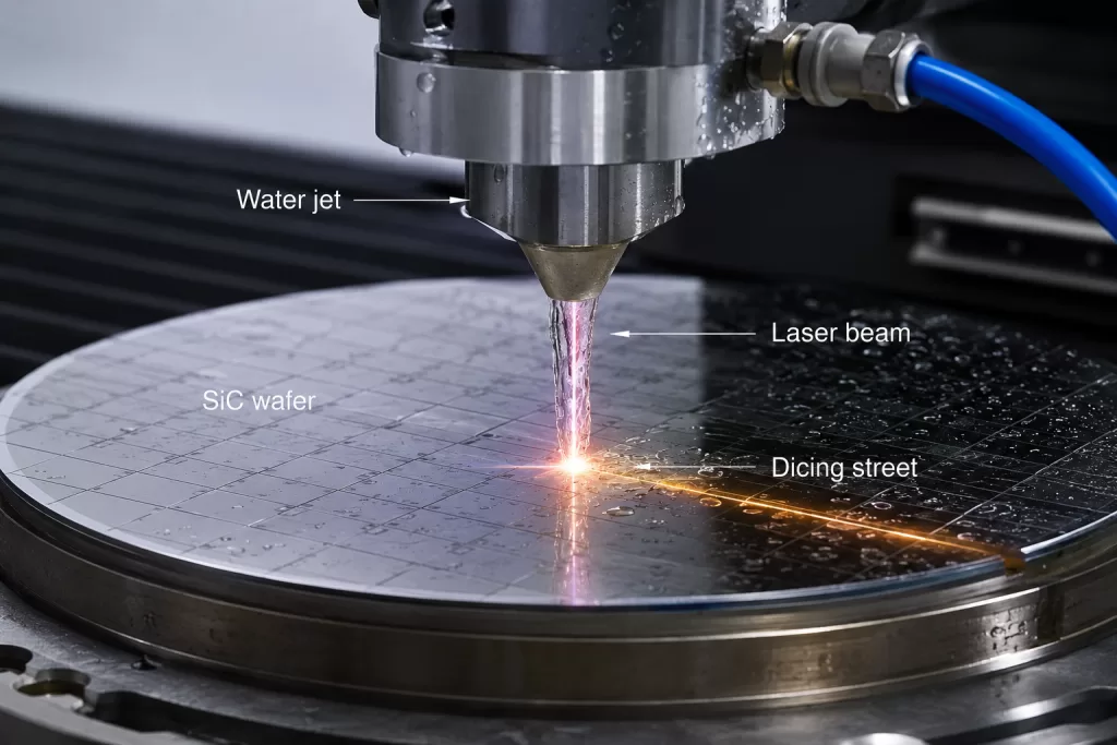
5. Water-jet Guided Laser Dicing
This method uses a thin water jet as a laser transmission medium.
Working Principle
Laser light is guided through a high-speed water micro-jet via total internal reflection, forming a stable beam that interacts with the wafer surface.
Avantages
- Reduced thermal damage compared to pure laser ablation
- Improved cutting quality
Limitations
- Limited processing speed
- Technical constraints for large-diameter wafers
- Effective mainly for wafers ≤ 6 inches in current industrial applications
6. Water Jet Assisted Laser Cutting
Unlike water-guided laser systems, this method uses a separate (non-coaxial) water jet combined with laser irradiation.
Characteristics
- Reduces thermal accumulation
- Improves edge quality compared to dry laser cutting
Limitations
- Low industrial adoption
- Complex system integration
- Limited processing efficiency
This technology is still under active development, primarily in research institutions and specialized equipment companies.
7. Laser Thermal Stress Cleaving (Thermal Cracking Method)
Working Principle
This method uses controlled thermal gradients:
- Laser irradiation generates localized heating and compressive stress
- Thermal diffusion creates temperature gradients
- Tensile stress develops inside the material
- Cracks propagate once stress exceeds material strength
Avantages
- Potential for controlled crack propagation
- No full material removal required
Limitations
- Crack stability is difficult to control
- Process sensitivity is high
- Limited industrial scalability
8. Laser Stealth Dicing (Internal Modification Dicing)
Laser internal modification is considered one of the most promising next-generation technologies.
Working Principle
A pulsed laser is focused inside the SiC wafer, forming a modified layer composed of:
- Microvoids
- High dislocation density regions
- Microcracks
This internal layer acts as a controlled fracture initiation plane. External force is then applied to separate the wafer.
Caractéristiques principales
- Minimal surface damage
- High precision cutting
- Low thermal impact due to ultrafast laser pulses
- Suitable for thin and thick wafers (multi-layer modification for ~350 μm wafers)
Avantages
- High cutting accuracy
- Excellent surface quality
- Reduced kerf loss
- High potential for industrial scaling
Future Potential
This method is widely regarded as a leading candidate for next-generation SiC wafer dicing technology.
9. Technology Comparison Table
| Méthode | Cutting Speed | Damage Level | Tool Wear | Precision | Industrial Maturity |
|---|---|---|---|---|---|
| Diamond Blade Dicing | Moyen | Haut | Haut | Moyen | Très élevé |
| Laser Ablation | Très élevé | High (thermal) | Aucun | Moyen | Haut |
| Water-jet Laser | Faible | Faible | Aucun | Haut | Moyen |
| Water Jet Assisted Laser | Low–Medium | Faible | Aucun | Haut | Faible |
| Thermal Cracking | Moyen | Moyen | Aucun | Moyen | Research Stage |
| Laser Stealth Dicing | Haut | Très faible | Aucun | Très élevé | Rapid Growth |
10. Future Trends in SiC Wafer Dicing
The future development of SiC wafer cutting technologies is moving toward:
- Ultra-short pulse laser processing
- Non-contact and low-damage dicing
- Higher wafer utilization efficiency
- Narrower kerf widths
- Multi-layer laser modification techniques
Among all methods, laser internal modification (stealth dicing) shows the strongest potential to become the mainstream industrial solution due to its balance of speed, precision, and low damage.
11. Conclusion
SiC wafer dicing is one of the most critical and technically challenging steps in semiconductor manufacturing. While traditional diamond blade dicing still dominates industrial production, laser-based and hybrid technologies are rapidly evolving.
In the long term, advanced laser dicing technologies—especially stealth dicing—are expected to redefine SiC wafer singulation by enabling:
- Rendement plus élevé
- Lower cost
- Improved device reliability