
Silicon Carbide has emerged as one of the most important wide-bandgap semiconductor materials in modern power electronics and high-temperature applications. Compared with conventional semiconductor materials such as Silicon, SiC offers superior electrical, thermal, and mechanical properties, enabling the development of high-efficiency devices for electric vehicles, renewable energy systems, and high-frequency power electronics.
However, producing high-purity SiC crystals suitable for semiconductor devices is extremely challenging. Crystal growth requires strict control of temperature, pressure, impurities, and defect formation. As a result, precision manufacturing standards have become a key factor in ensuring the quality, reliability, and scalability of SiC wafers.
This article provides an overview of high-purity SiC crystal growth technologies and the precision manufacturing standards that guide the production of semiconductor-grade SiC substrates.
Why High-Purity SiC Crystals Matter
The performance of SiC power devices largely depends on the quality of the underlying crystal substrate. Even small imperfections in the crystal structure can significantly affect device efficiency and reliability.
Key requirements for semiconductor-grade SiC crystals include:
| Parameter | Typical Requirement |
|---|---|
| Chemical purity | ≥ 99.9999% (6N) |
| Micropipe density | < 1 cm⁻² |
| Dislocation density | < 10⁴ cm⁻² |
| Wafer diameter | 100 mm – 200 mm (4–8 inch) |
| Surface roughness | < 0.5 nm (after polishing) |
High-purity SiC crystals allow manufacturers to fabricate advanced devices such as:
- SiC MOSFETs
- Schottky barrier diodes
- High-temperature sensors
- RF and microwave components
These devices are critical for improving power conversion efficiency in modern electronics.
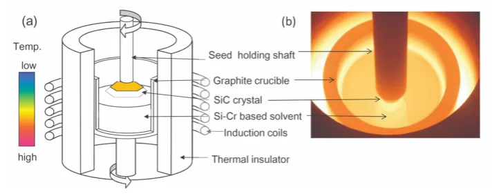
The Physical Vapor Transport (PVT) Growth Method
The most widely used method for growing bulk SiC crystals is the Physical Vapor Transport (PVT) technique, also known as the sublimation method.
Basic Process
In the PVT process:
- High-purity SiC powder is placed at the bottom of a graphite crucible.
- A seed crystal is mounted at the top of the crucible.
- The system is heated to 2000–2400 °C in an inert atmosphere, typically argon.
- The SiC powder sublimates into gaseous species.
- The vapor travels upward and recrystallizes on the seed crystal, forming a bulk SiC ingot.
This process enables controlled growth of large single crystals while maintaining the necessary purity levels for semiconductor applications.
Key Advantages
- High crystal purity
- Relatively stable growth environment
- Scalable to larger wafer diameters
- Compatible with industrial production
Despite these advantages, maintaining consistent crystal quality requires strict manufacturing control.
Precision Manufacturing Standards in SiC Crystal Growth
Modern SiC crystal growth relies on a combination of materials engineering, thermal management, and process monitoring. Several precision standards must be maintained throughout production.
1. Ultra-High Purity Raw Materials
Impurities such as aluminum, boron, and nitrogen can significantly alter the electrical properties of SiC. Therefore, raw materials used in crystal growth must meet extremely strict purity requirements.
Typical standards include:
- 6N or higher purity SiC source powder
- High-purity graphite crucibles
- Ultra-clean furnace environments
Contamination control is critical because even trace impurities can introduce deep-level defects in the crystal lattice.
2. Temperature Field Control
SiC crystal growth occurs at extremely high temperatures, making thermal stability one of the most important process parameters.
Precision control involves:
- Optimized furnace insulation design
- Multi-zone heating systems
- Controlled thermal gradients
A stable temperature gradient ensures uniform crystal growth and minimizes structural defects such as stacking faults and dislocations.
3. Defect Density Management
One of the major challenges in SiC manufacturing is controlling crystal defects. Common defects include:
- Micropipes
- Threading screw dislocations
- Basal plane dislocations
- Stacking faults
Advanced manufacturers implement several strategies to reduce defect density:
- High-quality seed crystal selection
- Optimized growth rates
- Real-time growth monitoring
Over the past two decades, defect densities have been dramatically reduced, enabling the commercialization of high-performance SiC devices.
4. Wafer Diameter and Scaling Standards
The semiconductor industry continually pushes for larger wafer sizes to improve manufacturing efficiency.
Current industrial standards include:
| Wafer Size | Typical Application |
|---|---|
| 4 inch (100 mm) | Research and early device production |
| 6 inch (150 mm) | Mainstream SiC device manufacturing |
| 8 inch (200 mm) | Next-generation high-volume production |
Scaling to 8-inch wafers presents additional challenges in maintaining uniform crystal quality across the entire substrate.
5. Surface Processing and Polishing
After crystal growth, the SiC ingot undergoes several processing steps:
- Crystal orientation measurement
- Wire-saw slicing
- Lapping
- Chemical-mechanical polishing (CMP)
These processes ensure that the final wafer meets strict semiconductor surface standards, including atomic-level smoothness and minimal subsurface damage.
Future Trends in SiC Crystal Manufacturing
As global demand for energy-efficient electronics continues to grow, SiC crystal manufacturing is evolving in several key directions.
Larger Wafer Production
The transition from 6-inch to 8-inch wafers is expected to significantly reduce device manufacturing costs.
Advanced Growth Monitoring
New technologies such as in-situ optical monitoring and AI-assisted furnace control are improving growth stability and yield.
Defect-Free Crystal Development
Research efforts are focused on producing near-zero defect SiC substrates, which would further enhance device performance and reliability.
Conclusion
High-purity SiC crystal growth represents one of the most demanding processes in semiconductor materials engineering. Through advanced growth techniques such as PVT, strict raw-material purification, and precise thermal control, manufacturers can produce high-quality SiC substrates that enable next-generation power electronics.
As industries move toward electrification and higher energy efficiency, precision manufacturing standards for SiC crystals will continue to evolve. Improvements in wafer size, defect control, and process automation will play a crucial role in supporting the expanding global market for SiC-based devices.