Silicon Carbide wafer Substrate’s abstract

Silicon Carbide (SiC) wafer substrates, renowned for their remarkable physical and chemical properties, have emerged as a revolutionary material in semiconductor technology. This abstract provides a comprehensive overview of the key attributes from both the physical and chemical perspectives, highlighting their implications in diverse applications.
Proprietà fisiche: Silicon Carbide boasts a distinctive set of physical properties that set it apart in the realm of semiconductor substrates.
- Ampio Bandgap: SiC exhibits a wide bandgap, a fundamental physical property critical for high-temperature and high-frequency applications. This wide bandgap contributes to its suitability for power electronics and optoelectronic devices.
- Conduttività termica: One of the standout features is its exceptional thermal conductivity. Silicon Carbide wafer Substrate efficiently dissipate heat, a crucial aspect in power devices where thermal management is a significant concern. This property enhances the overall efficiency and reliability of devices.
- Resistenza meccanica: Silicon Carbide possesses impressive mechanical strength, making it resistant to mechanical stress and wear. This characteristic ensures the durability and longevity of devices in demanding applications.
- High Breakdown Strength: Silicon Carbide wafer Substrate exhibit high breakdown strength, enabling the development of robust power devices with enhanced voltage capabilities. This is particularly advantageous in applications requiring high power and voltage.
- Temperature Stability: Silicon Carbide remains stable at elevated temperatures, demonstrating thermal stability and reliability. This makes it well-suited for applications in extreme environmental conditions, including automotive and aerospace systems.
Chemical Properties: The chemical properties of Silicon Carbide wafer Substrate contribute to their resilience and applicability in various environments.
- Inerzia chimica: Silicon Carbide is chemically inert, displaying resistance to corrosion and chemical reactions. This property ensures the stability and longevity of devices in corrosive or chemically aggressive environments.
- Resistance to Oxidation: Silicon Carbide wafer Substrate exhibit resistance to oxidation, a valuable trait in applications where exposure to oxygen and other oxidizing agents is prevalent. This resistance contributes to the material’s durability over time.
- Electronic Properties: Silicon Carbide’s electronic properties, influenced by its crystal structure, play a crucial role in its applications in the semiconductor industry. The material’s unique electronic band structure contributes to its performance in electronic and optoelectronic devices.
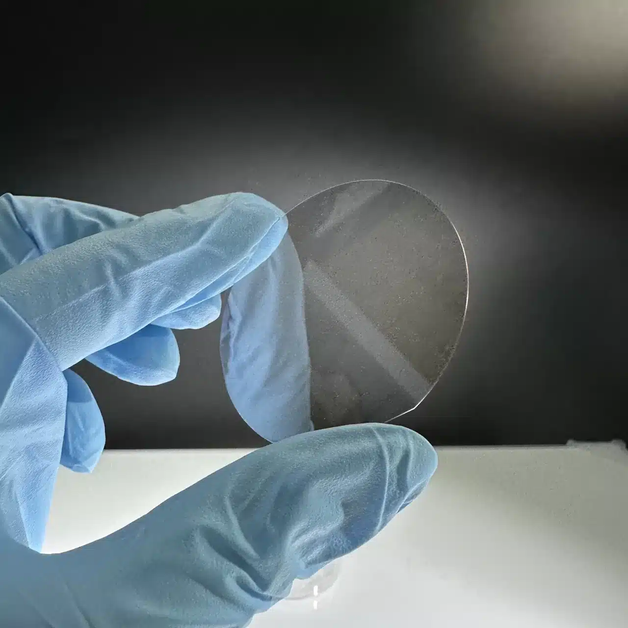
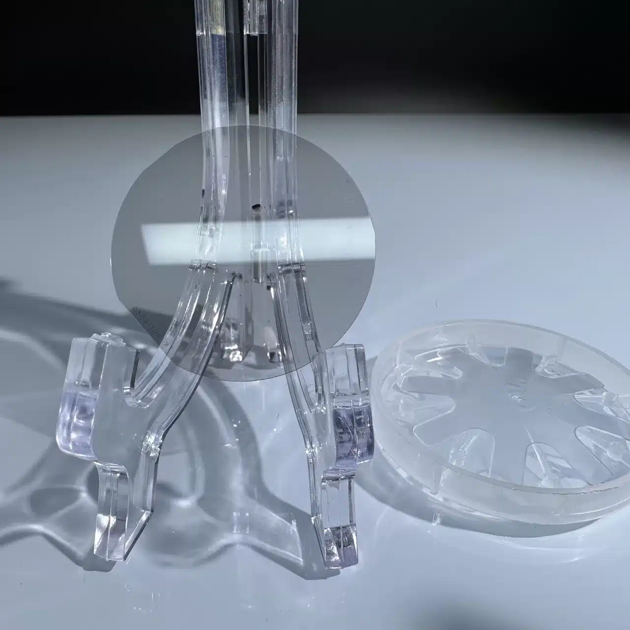
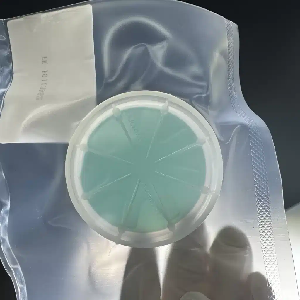
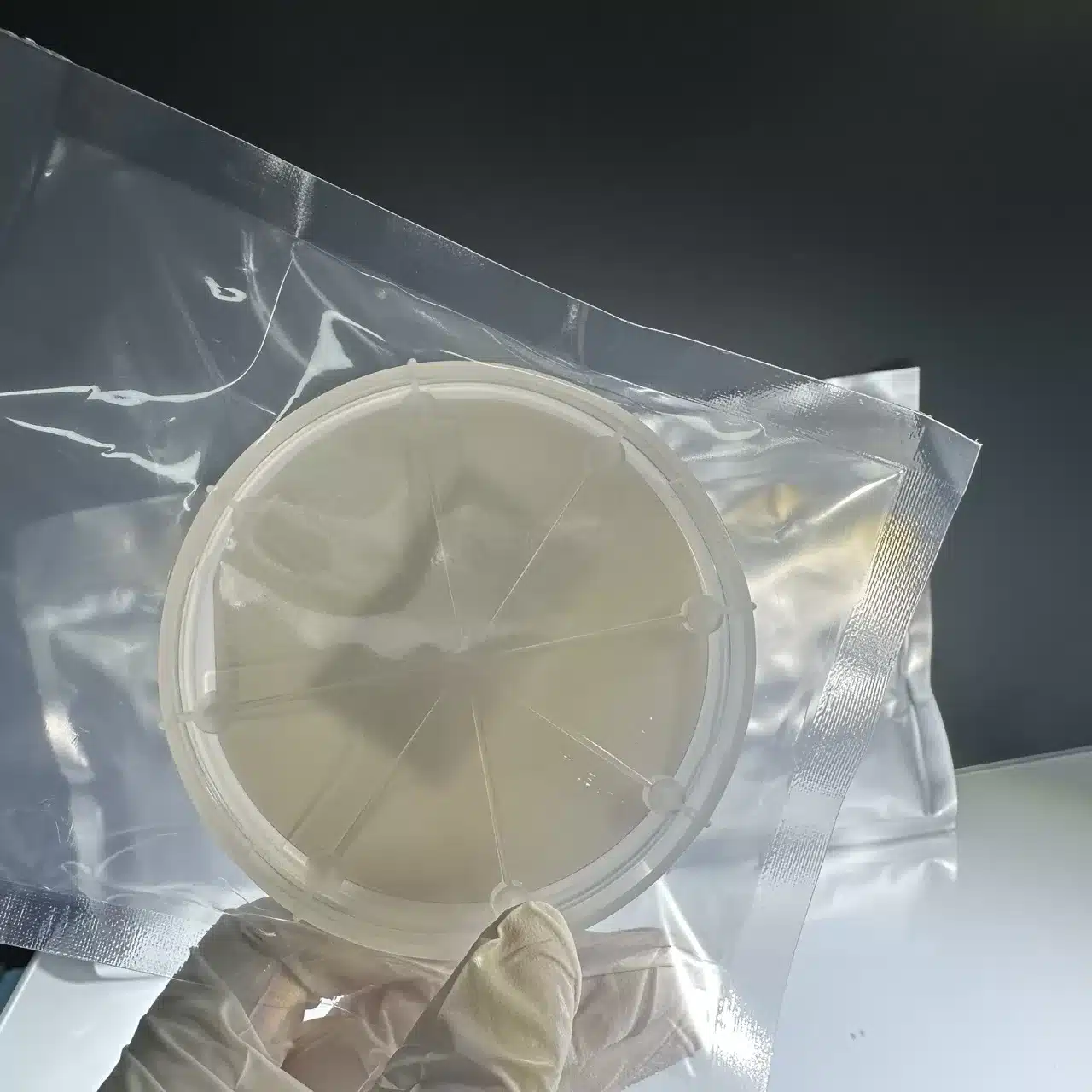
Silicon Carbide wafer Substrate that we can provide
2″ Carburo di silicio (SiC) 6H tipo N pronto per l'uso
2″ dia, 6H-N
Type/ Dopant : N / Nitrogen
Orientation : <0001>+/-0.5 degree
Thickness : 330 ± 25 um
D Grade,MPDä100 cm-2 D Grade,RT:0.02-0.2 Ω·cm
Single face polished/Si face epi-ready with Chemical Mechanical Polish (CMP),Surface Roughness : <0.5 nm
2″ 6H N-Type
6H-N 2″ dia, Type/ Dopant : N / Nitrogen
Orientation : <0001>+/-0.5 degree
Thickness : 330 ± 25 um
B Grade,MPDä30 cm-2 B Grade,RT 0.02 ~ 0.2 Ω·cm
Single face polished/Si face epi-ready with CMP,Surface Roughness : <0.5 nm

2″ Carburo di silicio (SiC) 4H tipo N pronto per l'uso
2″ 4H N-Type
4H-N 2″ dia, Type/ Dopant : N / Nitrogen
Orientation : <0001>+/-0.5 degree
Thickness : 330 ± 25 um
D Grade,MPDä100 cm-2 D Grade:RT:0.01-0.1 Ω·cm D Grade,Bow/Warp/TTV<25um
Single face polished/Si face epi-ready with CMP,Surface Roughness : <0.5 nm
2″ Silicon Carbide (SiC) 4H N-Type N-type Nitrogen Doped
4H-N 2″ dia, Type/ Dopant : N / Nitrogen
Orientation : <0001>+/-0.5 degree
Thickness : 330 ± 25 um
B Grade,MPDä30 cm-2 B Grade:RT:0.01 – 0.1 Ω·cm B Grade,Bow/Warp/TTV<25um
Single face polished/Si face epi-ready with CMP,Surface Roughness : <0.5 nm
3″ Carburo di silicio (SiC) 4H Tipo N
4H-N 3″ dia, Type/ Dopant : N / Nitrogen
Orientation :4 degree+/-0.5 degree
Thickness : 350 ± 25 um
D Grade,MPDä100 cm-2 D Grade,RT:0.01-0.1Ω·cm D Grade,Bow/Warp/TTV<35um
Double face polished/Si face epi-ready with CMP,Surface Roughness : <0.5 nm
3″ 4H N-Type
4H-N 3″ dia, Type/ Dopant : N / Nitrogen
Orientation : 4 degree+/-0.5 degree
Thickness : 350 ± 25 um
B Grade,MPDä30 cm-2 B Grade,RT:0.01 – 0.1Ω·cm B Grade,Bow/Warp/TTV<35um
Double face polished/Si face epi-ready with CMP,Surface Roughness : <0.5 nm
3″ 4H SI
4H-SI 3″ dia, Type/ Dopant : Semi-insulating / V
Orientation : <0001>+/-0.5 degree
Thickness : 350 ± 25 um
D Grade,MPDä100 cm-2 D Grade,RT:70 % ≥1E5 Ω·cm
Double face polished/Si face epi-ready with CMP,Surface Roughness : <0.5 nm
3″ 4H SI
4H-SI 3″ dia, Type/ Dopant : Semi-insulating / V
Orientation : <0001>+/-0.5 degree
Thickness : 350 ± 25 um
B Grade,MPDä30 cm-2 B Grade,RT:80 % ≥1E5 Ω·cm
Double face polished/Si face epi-ready with CMP,Surface Roughness : <0.5 nm
Silicon Carbide wafer Substrate’s application
Applications of Silicon Carbide Wafer Substrate in Sales and Beyond
Introduzione: Silicon Carbide (SiC) wafer substrates have become a cornerstone in various industries, offering unparalleled performance and versatility. This article explores the diverse applications of SiC wafers with a focus on how they drive sales and contribute to advancements in technology.
1. Elettronica di potenza: Silicon Carbide wafer Substrate play a pivotal role in the field of power electronics, driving innovations in devices such as Schottky diodes, Metal-Oxide-Semiconductor Field-Effect Transistors (MOSFETs), and power modules. The superior electrical properties, wide bandgap, and high thermal conductivity of SiC enable the development of high-power, high-efficiency electronic components.
2. Automotive Industry: The automotive sector benefits significantly from Silicon Carbide wafer Substrate applications. The robust nature of SiC wafers, combined with their high-temperature stability, positions them as essential components in electric vehicles (EVs) and hybrid electric vehicles (HEVs). SiC-based power devices contribute to increased energy efficiency and overall performance in automotive applications.
3. Aerospace and Defense: In aerospace and defense, SiC wafer substrates find crucial applications. The high breakdown strength and temperature stability of SiC make it indispensable for electronic components in aircraft and satellite technologies. SiC’s reliability in extreme conditions ensures the resilience of critical systems.
4. Optoelectronics: Silicon Carbide wafer Substrate contribute significantly to advancements in optoelectronic devices. Their unique properties make them ideal for use in light-emitting diodes (LEDs), photodetectors, and high-power lasers. SiC’s ability to withstand high temperatures enhances the reliability and performance of optoelectronic components.
5. Wireless Communication: SiC’s high-frequency capabilities make it suitable for wireless communication applications. SiC-based devices, leveraging the properties of Silicon Carbide wafer Substrate, contribute to the development of high-frequency transistors and amplifiers, enhancing communication systems.
6. Renewable Energy: Silicon Carbide wafer Substrate play a crucial role in the renewable energy sector, particularly in photovoltaic applications. SiC-based power devices are employed in solar inverters, enhancing the efficiency of solar energy conversion. This application aligns with the growing demand for sustainable energy solutions.
7. Research and Development: SiC wafer substrates serve as essential tools in research and development across various scientific disciplines. Their applications in experimental setups, sample preparation, and device prototyping contribute to advancements in materials science, physics, and electronics.
8. Semiconductor Manufacturing: The semiconductor industry relies on Silicon Carbide wafer Substrates for the production of cutting-edge electronic components. SiC’s unique combination of properties, including chemical inertness and high-temperature stability, contributes to the fabrication of reliable and high-performance semiconductor devices.
9. Medical Devices: SiC wafers find applications in the medical field, particularly in the manufacturing of precision medical devices. The high mechanical strength and biocompatibility of SiC contribute to the development of medical instruments used in surgeries and diagnostics.
10. Environmental Monitoring: SiC-based sensors, leveraging the properties of SiC wafers, are employed in environmental monitoring applications. These sensors provide accurate and reliable data in harsh conditions, contributing to environmental research and resource management.
Conclusione: The applications of Silicon Carbide wafer substrates extend across a myriad of industries, driving technological advancements and contributing to the evolution of various sectors. From powering electronic devices to enhancing communication systems and supporting renewable energy initiatives, SiC wafers play a vital role in shaping the future of technology. As industries continue to embrace the benefits of SiC, the demand for these versatile substrates is expected to grow, further solidifying their position as a key enabler of innovation and progress.
Silicon Carbide wafer Substrate’s partial data sheet
| Grado | Grado MPD zero | Grado di produzione | Grado di ricerca | Grado fittizio |
| Diametro | 50,6 mm±0,2 mm | |||
| Spessore | 1000±25um O altro spessore personalizzato | |||
| Orientamento del wafer | Fuori asse: 4,0° verso ±0,5° per 4H-N/4H-SI Sull'asse : ±0,5° per 6H-N/6H-SI/4H-N/4H-SI | |||
| Densità dei microtubi | ≤0 cm-2 | ≤2 cm-2 | ≤5 cm-2 | ≤30 cm-2 |
| Resistività 4H-N | 0,015~0,028 Ω-cm | |||
| Resistività 4/6H-SI | ≥1E7 Ω-cm | |||
| Primario Piatto | {10-10}±5,0° o forma rotonda | |||
| Lunghezza del piatto primario | 18,5 mm±2,0 mm o forma rotonda | |||
| Lunghezza del piano secondario | 10,0 mm±2,0 mm | |||
| Orientamento piatto secondario | Faccia di silicio rivolta verso l'alto: 90° CW. rispetto al primo piano ±5,0° | |||
| Esclusione dei bordi | 1 mm | |||
| TTV/Arcobaleno/Arcobaleno | ≤10μm /≤10μm /≤15μm | |||
| Ruvidità | Polacco Ra≤1 nm / CMP Ra≤0,5 nm | |||
| Crepe per luce ad alta intensità | Nessuno | 1 consentito, ≤2 mm | Lunghezza cumulativa ≤ 10 mm, lunghezza singola≤ 2 mm | |
| Piastre esagonali con luce ad alta intensità | Area cumulativa ≤1% | Area cumulativa ≤1% | Area cumulativa ≤3% | |
| Aree poliformi con luce ad alta intensità | Nessuno | Area cumulativa ≤2% | Area cumulativa ≤5% | |
| Graffi da luce ad alta intensità | 3 graffi a 1×diametro del wafer lunghezza cumulativa | 5 graffi a 1×diametro del wafer lunghezza cumulativa | 5 graffi a 1×diametro del wafer lunghezza cumulativa | |
| chip per bordi | Nessuno | 3 ammessi, ≤0,5 mm ciascuno | 5 consentiti, ≤1 mm ciascuno | |
Silicon Carbide wafer Substrate’s key feature
Unveiling the Key Features of Silicon Carbide Wafer Substrate
Introduzione: Silicon Carbide (SiC) wafer substrates have emerged as a transformative force in the semiconductor industry, showcasing a myriad of key features that set them apart in the realm of materials science. This comprehensive exploration aims to unveil the intrinsic attributes that define SiC wafer substrates, elucidating their significance in various applications and industries.
1. Wide Bandgap: A defining feature of SiC wafers is their wide bandgap, a crucial characteristic for applications requiring high-temperature and high-frequency performance. This property empowers the development of advanced electronic and optoelectronic devices, enhancing their efficiency and reliability.
2. High Thermal Conductivity: SiC wafers exhibit exceptional thermal conductivity, a pivotal factor in applications where efficient heat dissipation is paramount. This property enables the effective management of thermal loads, contributing to the longevity and optimal performance of devices, particularly in power electronics.
3. Mechanical Strength: Robust mechanical strength is inherent in SiC wafers, rendering them resistant to mechanical stress and wear. This feature ensures the durability and longevity of devices, making SiC a preferred choice for applications demanding structural integrity.
4. High Breakdown Strength: SiC wafers boast high breakdown strength, a critical attribute for the development of robust power devices with enhanced voltage capabilities. This feature enhances the reliability and resilience of devices, making them suitable for high-power applications.
5. Temperature Stability: The temperature stability of SiC wafers is a standout feature, enabling their use in extreme environmental conditions. This characteristic positions SiC as a material of choice for applications in automotive, aerospace, and other industries where elevated temperatures are encountered.
6. Chemical Inertness: SiC wafers exhibit chemical inertness, showcasing resistance to corrosion and chemical reactions. This property ensures the stability and longevity of devices in challenging environments, making SiC well-suited for applications in harsh or corrosive conditions.
7. Resistance to Oxidation: SiC wafers demonstrate resistance to oxidation, enhancing their durability over time. This resistance is particularly valuable in applications where exposure to oxygen and other oxidizing agents is prevalent, contributing to the longevity of SiC-based devices.
8. Crystal Structure and Electronic Properties: The crystal structure of SiC wafers influences their electronic properties, playing a crucial role in their performance in semiconductor devices. SiC’s unique electronic band structure contributes to its suitability for advanced electronic and optoelectronic applications.
9. Versatility in Applications: SiC wafers find extensive applications across diverse industries, including power electronics, automotive, aerospace, optoelectronics, and more. Their versatility stems from a harmonious combination of physical and chemical properties, making them an indispensable material in the technological landscape.
10. Contribution to Innovation: The key features of SiC wafers collectively contribute to their role as catalysts for innovation. Their application in cutting-edge technologies, such as electric vehicles, renewable energy systems, and high-frequency communication devices, highlights their transformative impact on the trajectory of technological advancement.
Conclusione: In conclusion, the key features of Silicon Carbide wafer substrates position them as a cornerstone in materials science and semiconductor technology. From their wide bandgap and high thermal conductivity to mechanical strength and chemical inertness, SiC wafers embody a spectrum of attributes that redefine the possibilities in various industries. As research and development in SiC technology continue, the multifaceted nature of these key features ensures SiC wafers will continue to play a pivotal role in shaping the future of electronic and optoelectronic devices.
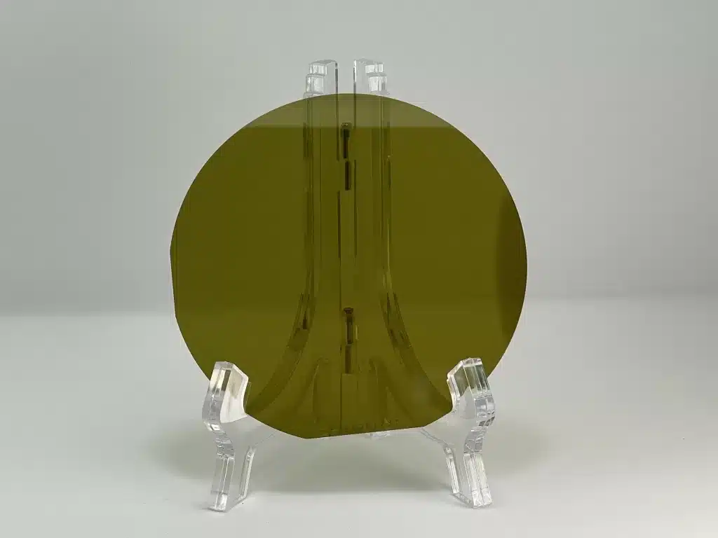
Silicon Carbide wafer Substrate’s showcase