ニュース
オリオンメタ・ガラス用SiC材料:光学的および熱的利点
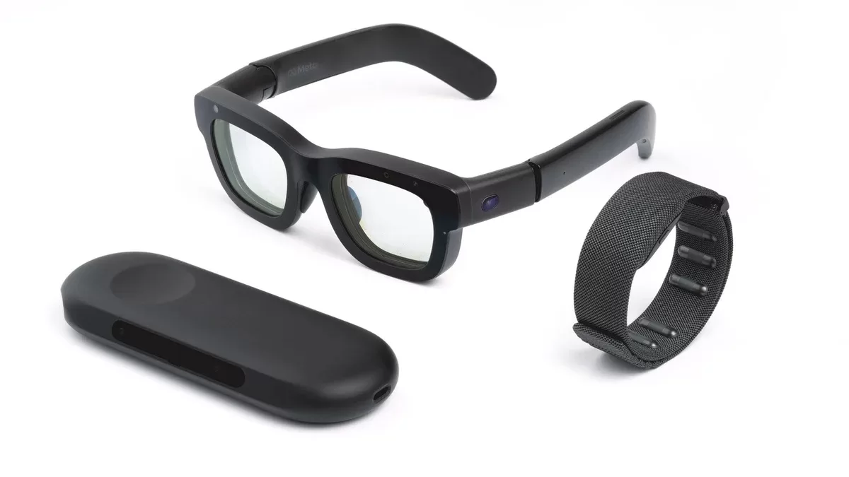
拡張現実(AR)とウェアラブル・ディスプレイ技術の急速な発展は、光学材料にかつてない要求を突きつけている。実験的なメタ・オリオンのような装置

拡張現実(AR)とウェアラブル・ディスプレイ技術の急速な発展は、光学材料にかつてない要求を突きつけている。実験的なメタ・オリオンのような装置
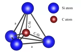
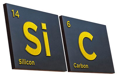
現代のパワーエレクトロニクスにおいて、炭化ケイ素は最も重要なワイドバンドギャップ半導体材料の一つとなっている。従来のシリコンに比べ、SiCは以下のような優れた特性を備えている。
産業オートメーションの進歩に伴い、製造、ロジスティクス、スマート生産ラインにおける高性能機器への需要が著しく高まっている。このようなシステムには、精密な
Silicon carbide (SiC) wafers have become a critical material for high-power electronics, electric vehicles, and advanced semiconductor devices. As the demand for higher efficiency, smaller
Silicon carbide (SiC) has emerged as a cornerstone material for high-power electronics, electric vehicles, and next-generation semiconductor devices due to its exceptional thermal conductivity, high
炭化ケイ素(SiC)パワーデバイスは、世界のパワーエレクトロニクス市場で急速にシェアを拡大している。従来のシリコンの物理的性能限界を超えることで
Silicon carbide (SiC) wafers, a core substrate for third-generation semiconductors, are rapidly becoming essential in high-performance power electronics and next-generation devices. Thanks to their superior
In modern industrial, automotive, and aerospace applications, the demand for sensors capable of operating reliably in high-temperature environments is rapidly increasing. Conventional silicon (Si) sensors,