ニュース
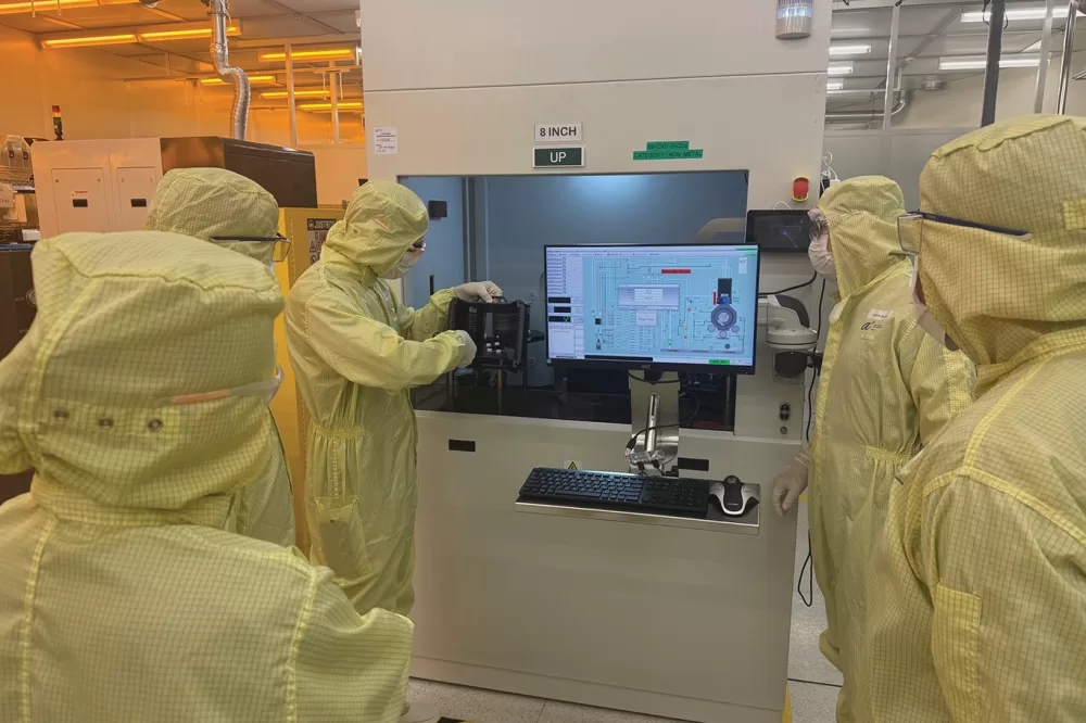
300mm対200mm SiCウェーハのコスト分析:12インチ化はどの程度の生産量で採算が合うのか?
Silicon carbide (SiC) wafers have become a critical material for high-power electronics, electric vehicles, and advanced semiconductor devices. As the demand for higher efficiency, smaller

Silicon carbide (SiC) wafers have become a critical material for high-power electronics, electric vehicles, and advanced semiconductor devices. As the demand for higher efficiency, smaller
炭化ケイ素(SiC)パワーデバイスは、世界のパワーエレクトロニクス市場で急速にシェアを拡大している。従来のシリコンの物理的性能限界を超えることで
炭化ケイ素(SiC)は、ニッチなワイドバンドギャップ材料から、次世代パワーエレクトロニクスの戦略的基盤へと急速に移行している。電気自動車への採用が加速する中,
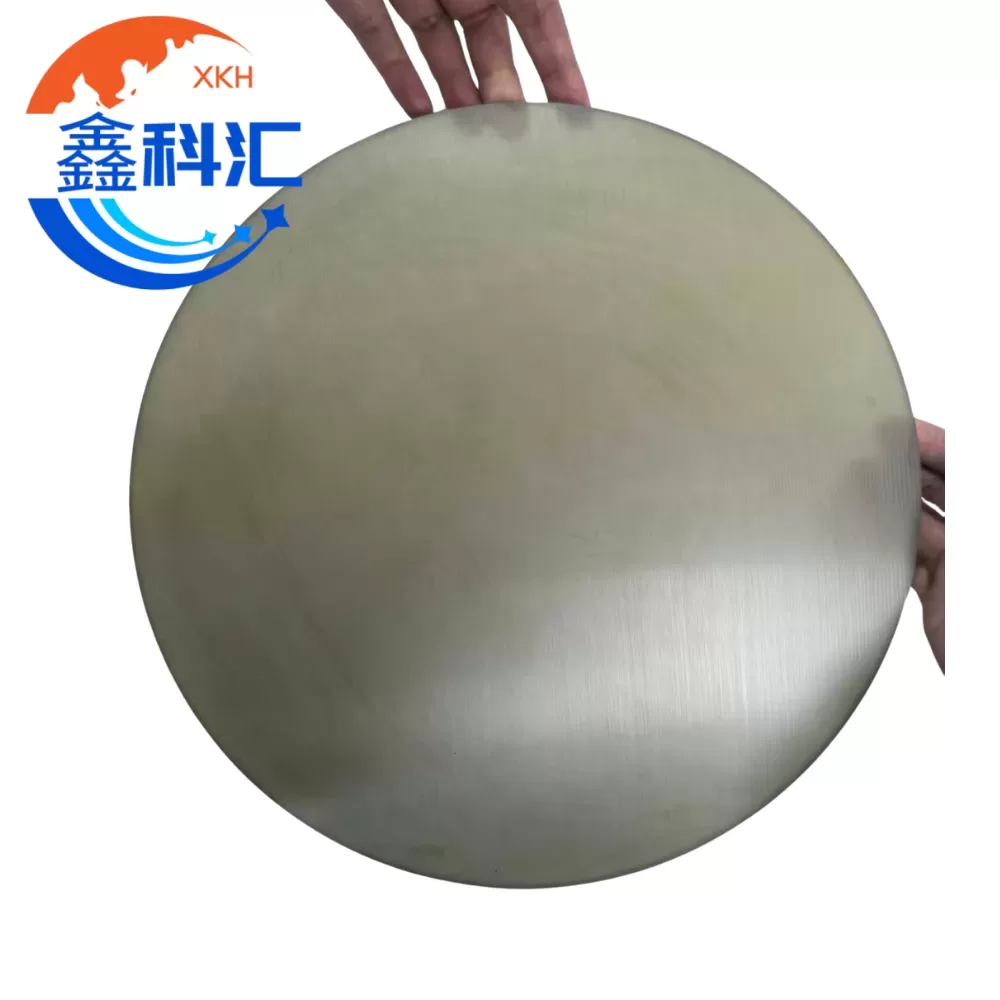
炭化ケイ素(SiC)基板は、その優れた熱伝導性、高ブレークダウン電界、優れた耐熱性により、次世代パワーエレクトロニクスの基盤材料として浮上している。
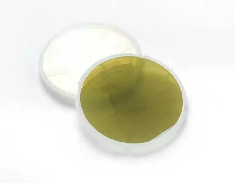
炭化ケイ素(SiC)ウェーハは、特に電気自動車、再生可能エネルギーシステム、急速充電器、および、電子機器などの高出力、高周波、高温エレクトロニクスの基礎材料となっている。

炭化ケイ素(SiC)は、ハイパワーエレクトロニクス、高周波デバイス、過酷な環境下での応用において、基幹材料として浮上してきた。その優れた熱伝導性、高耐圧、そして
With the rapid development of electric vehicles, 5G base stations, and renewable energy power electronics, substrate selection has become a critical factor in high-power device
Silicon carbide (SiC) wafers have become a cornerstone material in power electronics, automotive, and high-frequency applications due to their superior breakdown electric field, thermal conductivity,