
Why Global Demand for SiC Wafers Continues to Grow Across EV, Renewable Energy and Industrial Electronics

Silicon carbide wafers have moved from a specialized semiconductor material to a strategically important foundation for modern power electronics. The strongest demand comes from electric vehicles, renewable energy infrastructure and industrial electronic systems. These sectors all face a similar engineering challenge: they must control increasingly large amounts of electrical power while reducing energy losses, thermal […]
Future Trends in SiC Wafer Manufacturing: Larger Diameters, Lower Defect Density and Higher Yield
Silicon carbide (SiC) has become one of the most important semiconductor materials for next-generation power electronics. Compared with conventional silicon, SiC offers a wider bandgap, higher critical electric field, greater thermal conductivity and superior high-temperature performance, making it the preferred material for electric vehicles (EVs), renewable energy systems, industrial motor drives, rail transportation and aerospace […]
SiC Wafer Manufacturing Challenges: Crystal Growth, Slicing, and Polishing
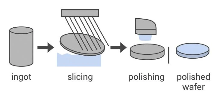
Silicon Carbide (SiC) has emerged as one of the most important semiconductor materials for next-generation power electronics. Thanks to its wide bandgap, high thermal conductivity, and superior breakdown electric field, SiC devices offer significant advantages over traditional silicon-based technologies in electric vehicles, renewable energy systems, industrial drives, and high-voltage power conversion. Despite these advantages, manufacturing […]
Common Defects in SiC Wafer and Their Impact on Device Performance
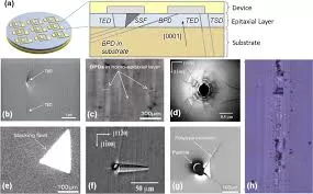
Silicon Carbide (SiC), as a third-generation wide-bandgap semiconductor material, has gained significant importance in power electronics, including electric vehicles, photovoltaic inverters, high-voltage power supplies, and industrial energy systems. Thanks to its wide bandgap, high breakdown electric field, and excellent thermal conductivity, SiC enables devices with higher efficiency, higher switching speed, and better high-temperature stability compared […]
Silicon Carbide Is Entering the AI Era: From EV Power Devices to AI Infrastructure Materials
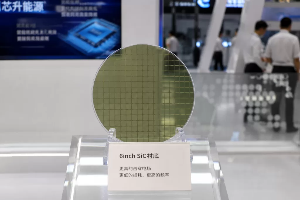
For years, silicon carbide (SiC) has been viewed primarily as a “new energy material” tied to electric vehicles, solar inverters, and industrial power electronics. But the market narrative is changing rapidly. With the explosive growth of AI computing infrastructure, silicon carbide is becoming a foundational material for next-generation power delivery, advanced packaging, and thermal management […]
N-Type vs. Semi-Insulating SiC Wafers: Main Differences and Applications
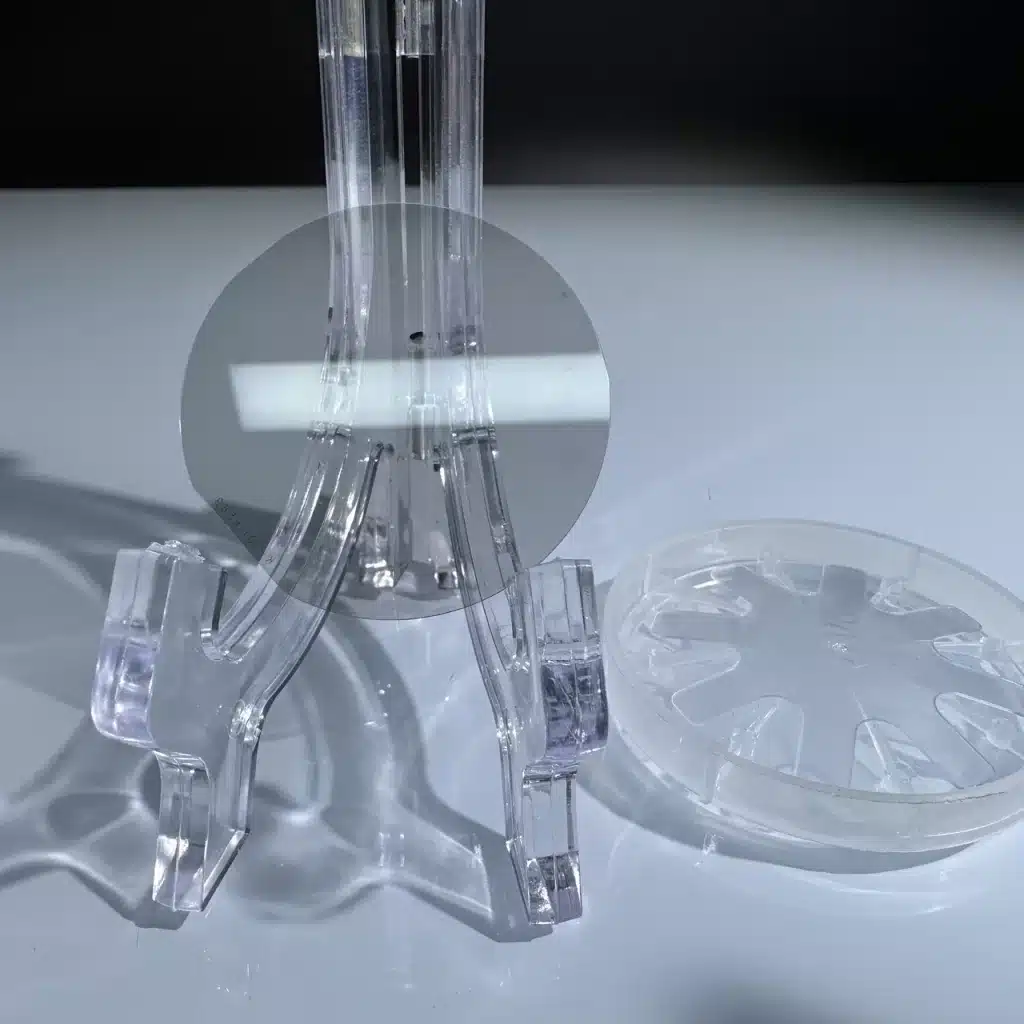
Silicon carbide (SiC) wafers have become one of the most important wide-bandgap semiconductor substrates in power electronics, RF communication, and high-temperature applications. Among the most widely used types are N-type SiC wafers and semi-insulating SiC wafers. Although they may look similar physically, their electrical behavior and application fields are fundamentally different. Choosing the wrong type […]
SiC Wafer Specification Guide: Polytype, Doping, Micropipes and How to Choose
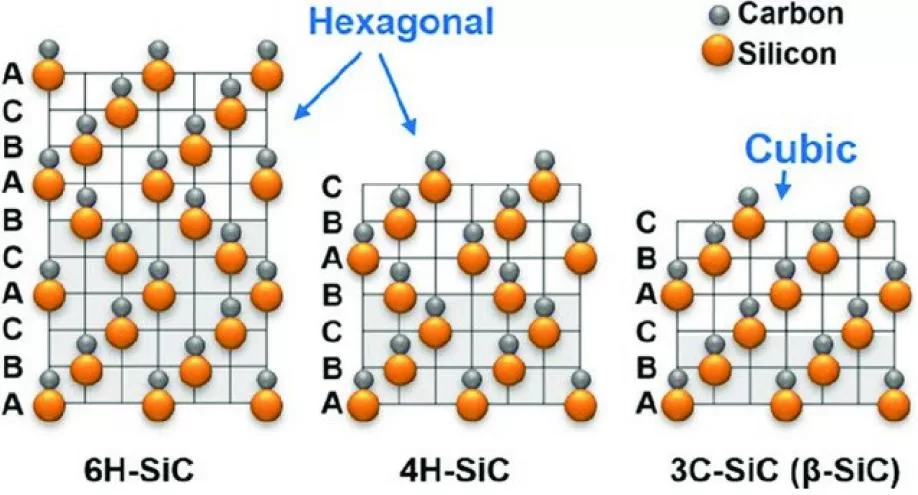
1. Introduction Silicon carbide (SiC) has become a cornerstone material in power electronics, RF devices, and harsh-environment applications due to its wide bandgap, high thermal conductivity, and exceptional breakdown field. However, unlike silicon, SiC wafer selection is highly non-trivial. Subtle differences in polytype, doping, and defect density can directly determine device performance, yield, and long-term […]
300mm Wafer vs 200mm Wafer: Key Differences and Use Cases
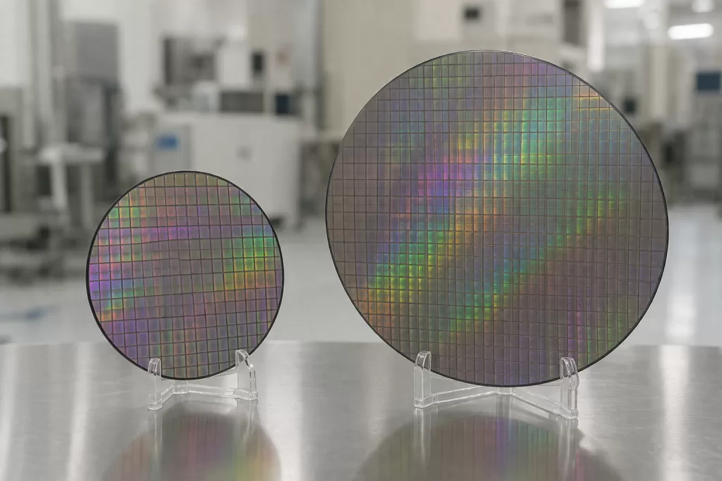
1. Introduction In modern semiconductor manufacturing, wafer size plays a critical role in determining production efficiency, device performance, and overall cost structure. Among the most widely used wafer formats, 200mm (8-inch) and 300mm (12-inch) wafers represent two major generations of fabrication technology. While 200mm wafers remain essential in legacy and specialized applications, 300mm wafers dominate […]