ニュース
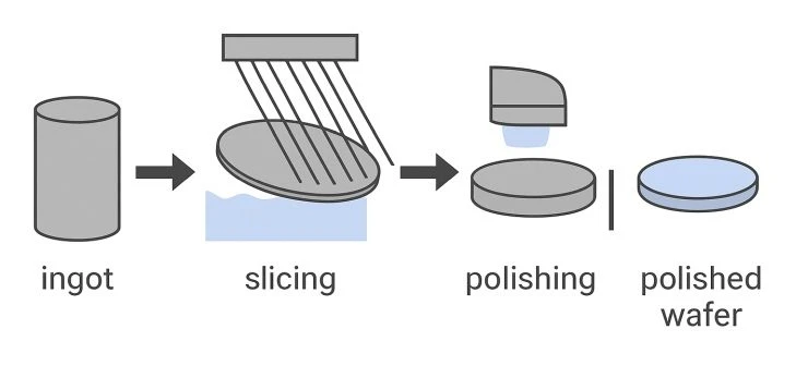
SiCウェハーの製造における課題:結晶成長、スライシング、および研磨
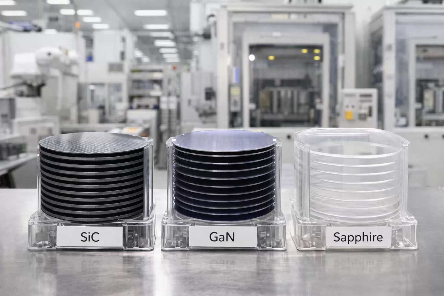
Silicon Carbide (SiC) has emerged as one of the most important semiconductor materials for next-generation power electronics. Thanks to its wide bandgap, high thermal conductivity,

Silicon Carbide (SiC) has emerged as one of the most important semiconductor materials for next-generation power electronics. Thanks to its wide bandgap, high thermal conductivity,
Silicon Carbide (SiC), as a third-generation wide-bandgap semiconductor material, has gained significant importance in power electronics, including electric vehicles, photovoltaic inverters, high-voltage power supplies, and

As semiconductor technology advances toward smaller process nodes, larger wafer sizes, and increasingly complex manufacturing environments, material selection has become a critical engineering consideration. Modern
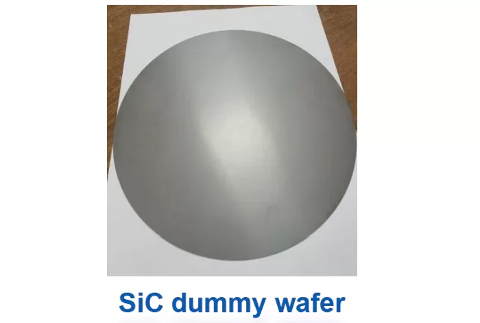
1. Introduction In semiconductor manufacturing, a dummy wafer (also known as a monitor wafer or blank wafer) is a non-device-bearing wafer used to support and
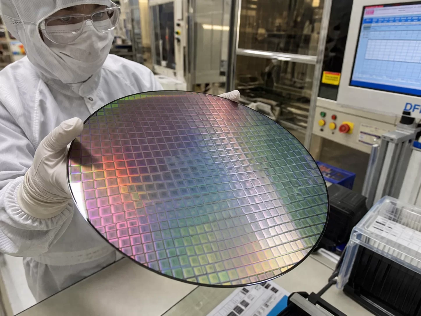
インテルのSkylakeシリーズに代表される最新のマイクロプロセッサの生産は、大きなシリコンウェハーから始まる。1枚のウェハーから何個のチップを生産できるかを理解することは、次のことを意味する。
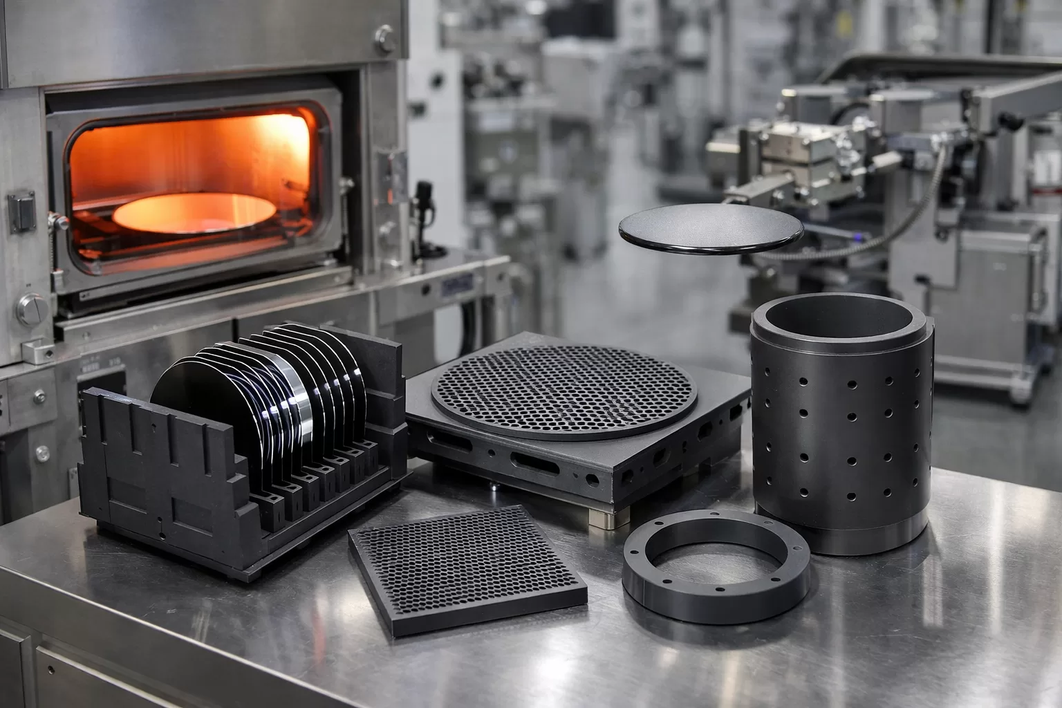
先進的な製造システムでは、歩留まり、安定性、長期的性能の真の決定要因は、多くの場合、ヘッドライン・マシンではなく、その下で静かに作動する材料である。
1.はじめに シリコンは、その豊富さ、安定した結晶構造、優れた電子特性により、数十年にわたり半導体産業を支配してきた。しかし、デバイスの微細化に伴い
Silicon carbide (SiC) wafers have become a critical material for high-power electronics, electric vehicles, and advanced semiconductor devices. As the demand for higher efficiency, smaller