
Key words:P Grade SiC Substrate,8-inch N-type SiC,8-inch SiC Wafer,N-type Silicon Carbide Crystal,SiC Power Device Substrate,SiC Crystal P Grade
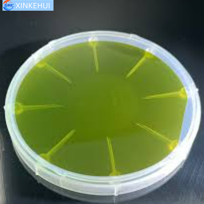
P Grade 8inch N type SiC substrate ‘s abstratct
について 8-inch P Grade N-type SiC Substrate is a high-performance silicon carbide crystal substrate designed specifically for demanding power applications. Known for its high conductivity, this 8-inch N-type SiC for power devices provides exceptional thermal management and reliability, making it an ideal choice for high-voltage and high-temperature environments. Engineered as a P Grade 8-inch N-type SiC Wafer, this substrate offers superior purity and precision, ensuring efficient energy handling in critical applications.
Utilized in sectors like electric vehicles and industrial power, this 8-inch Silicon Carbide Power Device Substrate supports robust power conversion systems by maintaining stability even under extreme conditions. Its high purity そして N-type conductivity optimize it for power semiconductors, ensuring minimal energy loss and enhanced device longevity. As a P Grade SiC Crystal for electric vehicles, it’s instrumental in reducing power inefficiencies, supporting sustainable energy solutions.
Overall, the P Grade 8-inch N-type SiC Wafer is not only a foundation for next-generation power electronics but also a versatile 8-inch SiC for power semiconductors that addresses the rigorous demands of modern power device applications.
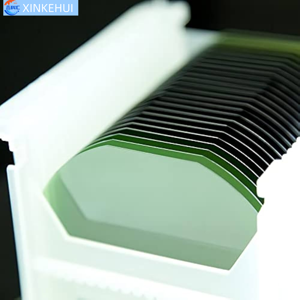
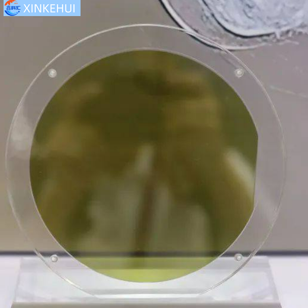
P Grade 8inch N type SiC substrate ‘s specification
| P grade N type SiC Crystal Parameters | |
| Polytype | 4H |
| Polytype Area | None Permitted |
| マイクロパイプ密度 | -2 ≤1 cm |
| Hex Plates | None Permitted |
| Hexagonal Polycrystalline | None Permitted |
| Inclusion | area≤0.05% |
| 抵抗率 | 0.015Ω•cm—0.025Ω•cm |
| 通常版 | ≤8000 cm-2 |
| TED | ≤6000 cm-2 |
| BPD | ≤2000 cm-2 |
| TSD | ≤1000 cm-2 |
| SF | ≤1% |
| Metal Contamination | (Al, Cr, Fe, Ni, Cu, Zn, Pb, Na, K, Ti, Ca, V, Mn) ≤1E11 cm-2 |
| Mechanical Parameters | |
| 直径 | 200.0 mm+0mm/-0.5mm |
| Surface Orientation | 4°toward <11-20>±0.5° |
| プライマリー・フラットの長さ | Notch |
| セカンダリー・フラットの長さ | なし |
| Notch Orientation | <1-100>±1° |
| Notch Angle | 90° +5°/-1° |
| Notch Depth | 1mm +0.25mm/-0mm |
| Orthogonal Misorientation | ±5.0° |
| 表面仕上げ | C-Face: Optical Polish, Si-Face: CMP |
| Wafer Edge | Beveling |
| 表面粗さ (10μm×10μm) | Si-Face:Ra≤0.2 nm C-Face:Ra≤0.5 nm |
| 厚さ | 500.0μm±25.0μm |
| LTV (10mmx10mm) | ≤3μm |
| TTV | ≤10μm |
| 弓 | ≤25μm |
| Warp | ≤40μm |
| Surface Parameters | |
| Chips/Indents | None permitted≥0.5mm Width and Depth |
| a Scratches (Si face CS8520) | ≤5 and Cumulative Length≤ 1 Wafer Diameter |
| a TUA (2mm*2mm) | ≥95% |
| Cracks | None Permitted |
| Stain | None Permitted |
| Edge Exclusion | 3mm |
P Grade 8inch N type SiC substrate ‘s properties
Key Properties of P Grade 8-inch N-type SiC Substrate:
- Size and Dimensions
- 直径: 8 inches (approximately 200 mm)
- 厚さ: Typically around 350 micrometers, with precise control to support consistent manufacturing processes.
- Crystal Type
- Polytype: Available in both 4H-SiC and 6H-SiC configurations, depending on application needs, each offering specific properties in terms of electron mobility and thermal conductivity.
- Doping Type
- N-type: Enhanced with nitrogen doping, ideal for high-power and high-frequency applications.
- 電気的特性
- High Conductivity: P Grade 8inch N type SiC substrate Exhibits low electrical resistivity, supporting efficient current flow, which is crucial for power devices.
- Breakdown Electric Field: High breakdown voltage, allowing it to withstand high voltages without degrading performance.
- 熱特性
- 高い熱伝導性: Excellent heat dissipation capabilities, ensuring stable operation in high-temperature environments.
- 熱膨張係数😛 Grade 8inch N type SiC substrate Low coefficient ensures structural integrity under thermal cycling.
- Purity and Quality Grade
- P Grade: High purity, optimized for research and high-performance applications.
- マイクロパイプ密度: Typically less than 0.5 cm², minimizing defects and improving device longevity.
- アプリケーション
- Ideal for power devices in electric vehicles, renewable energy systems, industrial power supplies, and other high-performance semiconductor applications.
- 機械的特性
- 高硬度: P Grade 8inch N type SiC substrate High on the Mohs hardness scale (~9.2), offering durability and resilience in device fabrication and operation.
メリット
- Superior Reliability in high-stress environments, making it suitable for applications requiring consistent performance under extreme conditions.
- Extended Device Lifespan thanks to low defect rates and robust material integrity.
- Efficiency Boost: Lower energy losses and higher operating efficiency in power conversion systems.
These properties make the P Grade 8-inch N-type SiC substrate a top choice for next-generation power semiconductors, supporting innovations in energy-efficient, high-power electronic devices.
P Grade 8inch N type SiC substrate ‘s applications
1. Electric Vehicles (EVs)
- Power Modules and Inverters: In electric vehicle (EV) powertrains, P Grade 8-inch N-type SiC substrates are critical for power modules and inverters, which manage the conversion of energy between the vehicle’s battery and its electric motor. SiC substrates in these modules reduce switching losses and enhance power efficiency, allowing for more compact and lightweight designs, which is vital in optimizing EV range and reducing battery consumption.
- Onboard Chargers and Fast-Charging Stations: P Grade 8inch N type SiC substrateenable the high efficiency needed for onboard charging systems in EVs, supporting both standard and fast-charging capabilities. Their high thermal conductivity prevents overheating during rapid charging, extending component life and improving charging station efficiency, which is essential as EV infrastructure expands globally.
2. Renewable Energy Systems
- Solar Power Inverters: In photovoltaic (PV) solar systems, inverters convert DC power from solar panels into AC power for household or grid use. The high power density and thermal efficiency of 8-inch N-type SiC substrates help reduce losses in energy conversion, enhance system efficiency, and minimize heat generation, which reduces the need for complex cooling systems. This allows solar systems to operate with lower maintenance and greater energy yield, supporting the growth of renewable energy adoption.
- Wind Turbine Converters: Wind turbines generate fluctuating power that needs to be converted into a stable form before it’s fed into the grid. P Grade SiC substrates play a role in power electronics used for this purpose, allowing converters to handle high voltage loads with minimal energy losses. Their resistance to environmental stress makes them ideal for use in offshore wind farms where they endure harsh weather conditions.
3. Industrial Power Supplies
- High-Frequency Power Converters: Many industrial operations rely on high-frequency power converters to supply energy to heavy machinery and equipment. The P Grade 8-inch N-type SiC substrate is integral to these power converters, supporting higher switching frequencies, efficient energy conversion, and reduced heat dissipation. These properties improve the longevity of the equipment and allow for more compact, efficient designs, which are beneficial in space-constrained industrial settings.
- Motor Drives and Variable Frequency Drives (VFDs): In industries that require precise control over motors, such as manufacturing and automation, motor drives and VFDs play a crucial role. SiC基板 ensure that these devices can handle the intense, high-speed switching required to control motor speed and torque accurately. The SiC substrate’s durability also minimizes downtime and maintenance costs, providing long-term reliability in harsh operating environments.
4. Telecommunications
- 5G Base Stations😛 Grade 8inch N type SiC substrate As the demand for 5G infrastructure increases, power devices within base stations require materials that can support high frequencies and voltages without signal loss. P Grade 8inch N type SiC substratesubstrates are ideal for RF power amplifiers used in these stations, helping transmit signals more efficiently across large areas. Their high breakdown voltage ensures that base stations can handle high power loads, while their thermal efficiency reduces the need for elaborate cooling solutions.
- RF Power Amplifiers for Signal Processing: Beyond telecommunications, RF power amplifiers with SiC基板 are used in various sectors for signal processing, including aerospace, defense, and satellite communication. The high-quality P Grade 8inch N type SiC substrateprovides excellent signal integrity, high power density, and improved efficiency, enabling faster and more reliable communication technologies.
5. 航空宇宙・防衛
- Radar Systems: Military and civilian radar systems operate in challenging conditions and require highly reliable components. P Grade 8-inch N-type SiC substrates provide the needed durability and resilience, ensuring consistent signal processing even at high frequencies. This makes them essential in radar applications, from air traffic control to military surveillance, where reliability is paramount.
- Satellite and Spacecraft Power Systems: In satellite applications, power systems must function with minimal maintenance over extended periods. The P Grade 8inch N type SiC substrate resistance to high temperatures, radiation, and voltage fluctuations is invaluable, making it ideal for the power management modules in satellites. These properties allow satellites to maintain stable power supply even in extreme space environments, where consistent performance and longevity are critical.
6. 医療機器
- Advanced Imaging Systems (MRI, CT): Medical imaging devices such as MRI and CT scanners require high-power components to deliver accurate results. The high thermal conductivity of P Grade SiC substrates minimizes heat buildup, ensuring precise control over energy output and reducing noise interference in imaging processes. P Grade 8inch N type SiC substrate resulting enhanced image quality supports better diagnostics and patient care.
- Portable and Implantable Medical Devices: For portable devices that need efficient power management, P Grade 8inch N type SiC substrate support miniaturized designs and low power consumption. In implantable devices, SiC’s biocompatibility and high durability allow for reliable, long-lasting operation, which is essential for patient safety and health outcomes.
7. Data Centers and High-Performance Computing (HPC)
- Power Supply Modules and Cooling Systems: As data centers demand more computing power and high-performance computing (HPC) systems scale up, power density and cooling efficiency are critical. P Grade 8-inch N-type SiC substrates allow power supply modules to handle higher loads while dissipating less heat. This efficiency reduces the cooling requirements of data centers, leading to lower operating costs and reduced environmental impact.
- Uninterruptible Power Supplies (UPS)😛 Grade 8inch N type SiC substrate Data centers and HPC systems rely on UPS systems to prevent downtime during power outages. P Grade 8inch N type SiC substrate enable UPS systems to provide stable, efficient backup power and to switch between power sources with minimal energy loss, enhancing the resilience and uptime of these critical infrastructures.
8. コンシューマー・エレクトロニクス
- High-Power Chargers: With the increase in high-power devices, consumer electronics require compact yet efficient power supplies. P Grade SiC substrates are employed in chargers for laptops, gaming consoles, and mobile devices, allowing for faster charging with minimal heat generation.
- Home Energy Storage and Management Systems: Residential energy storage solutions integrate 8-inch SiC substrates to handle the power conversion processes from battery storage to home use. Their high efficiency and low thermal footprint help make home energy systems more compact, quieter, and more energy-efficient.
9. Railway and Public Transport Systems
- Traction Control and Inverters: Railway systems and electric buses require efficient traction control systems to manage power distribution effectively. P Grade 8-inch N-type SiC substrates play an important role in these inverters, providing the high power density needed to maintain speed and reliability. P Grade 8inch N type SiC substrate translates to lower energy consumption and fewer emissions, aligning with the shift toward greener public transportation systems.
- Auxiliary Power Systems: P Grade 8inch N type SiC substrate Auxiliary power supplies, which provide electricity for lighting, HVAC, and control systems in public transportation, benefit fromP Grade 8inch N type SiC substrate due to their high efficiency and compactness, reducing overall vehicle weight and improving energy efficiency.
10. Smart Grid Infrastructure
- Energy Conversion and Distribution: Smart grids require advanced power management systems to optimize energy distribution across different regions. P Grade 8inch N type SiC substrate support the design of highly efficient energy converters and inverters, helping improve power quality, reduce energy losses, and stabilize grid performance.
- Grid-Connected Storage Solutions: To stabilize grid load and manage peak demands, P Grade 8inch N type SiC substrate -based inverters and converters are integrated with grid-connected battery storage systems. The P Grade 8inch N type SiC substrate ensures these systems are energy-efficient, reliable, and capable of handling large-scale power transfers.
RFQ for P Grade 8inch N type SiC substrate
What is P Grade 8inch N type SiC substrate?
について P Grade 8-inch N-type SiC substrate is a high-purity silicon carbide (SiC) substrate specifically designed for power and high-frequency semiconductor applications. Here’s a breakdown of what each part of the name represents:
- P Grade: Indicates a high purity or quality level. “P Grade” SiC substrates are usually free from major defects, have low micropipe densities, and meet stringent quality standards, making them suitable for advanced research, power electronics, and high-reliability applications.
- 8-inch: Refers to the diameter of the substrate, which is approximately 200 mm. An 8-inch diameter allows for larger wafers, which can support more devices or larger power devices, increasing manufacturing efficiency and reducing costs per unit.
- N-type: This is the type of doping applied to the SiC substrate. N-type doping means that the silicon carbide is doped with nitrogen, adding extra electrons to the crystal lattice and making it suitable for applications that require high conductivity, such as power devices.
- SiC (Silicon Carbide): Silicon carbide is a compound of silicon and carbon known for its exceptional thermal conductivity, high breakdown electric field, and mechanical strength. These characteristics make SiC ideal for high-temperature and high-voltage applications where traditional silicon substrates might fail.
What is n type SiC?
N-type SiC (N-type silicon carbide) refers to silicon carbide (SiC) that has been doped to have an excess of electrons, making it electrically conductive. In N-type SiC, doping is typically achieved by introducing nitrogen atoms into the silicon carbide crystal structure. Here’s a breakdown of what makes N-type SiC unique:
Key Features of N-type SiC
- Doping with Nitrogen: In the SiC crystal lattice, nitrogen atoms substitute for some of the silicon or carbon atoms. Nitrogen has more electrons than silicon or carbon, resulting in an excess of free electrons in the lattice. These free electrons make the material electrically conductive, allowing it to carry current effectively.
- High Electron Mobility: N-type SiC has high electron mobility, meaning that electrons can move quickly through the material. This property is beneficial for high-frequency and high-power applications, where efficient electron flow is crucial.
- Thermal and Mechanical Stability: Like other forms of SiC, N-type SiC maintains its performance even at high temperatures and in harsh environments. Its excellent thermal conductivity helps in dissipating heat, which is essential for high-power devices.
- High Breakdown Voltage: N-type SiC can withstand high electric fields before it breaks down, making it suitable for power devices that operate at high voltages.
Applications of N-type SiC
Because of its ability to conduct current and withstand high temperatures and voltages, N-type SiC is widely used in power electronics, high-frequency devices, そして high-temperature applications. Some specific applications include:
- パワーデバイス: Used in MOSFETs, diodes, and other semiconductor components for efficient power conversion in electric vehicles, renewable energy systems, and industrial machinery.
- RF and Microwave Applications: Suitable for RF amplifiers and communication systems due to its high-frequency capability.
- High-Voltage Switches and Converters: Ideal for power supplies, inverters, and converters that need to handle high voltages with minimal energy loss.
In summary, N-type SiC is a doped form of silicon carbide that is optimized for electrical conductivity, making it a valuable material for devices requiring high efficiency, durability, and reliability under extreme conditions.
What is the difference between SiO2 and SiC?
SiO₂ (Silicon Dioxide) そして SiC (Silicon Carbide) are both materials widely used in various industrial applications, but they have fundamentally different properties and are used for different purposes due to their unique chemical compositions and physical characteristics. Here are the key differences:
1. 化学組成
- SiO₂ (Silicon Dioxide): Composed of one silicon atom bonded to two oxygen atoms. It is commonly found in nature as quartz and in various forms of sand. SiO₂ is an insulating material.
- SiC (Silicon Carbide): Composed of one silicon atom bonded to one carbon atom, giving it unique properties distinct from those of SiO₂. SiC is a semiconducting material that is highly durable and conductive under certain conditions.
2. 電気的特性
- SiO₂: An electrical insulator with very high resistivity, commonly used as a dielectric material in electronics to provide insulation between conductive layers. It does not conduct electricity, making it ideal for use in gate oxides and as an insulator in semiconductor devices.
- SiC: A semiconductor with high thermal conductivity and high breakdown electric field. SiC is used in power electronics because it can operate under high voltages and temperatures, unlike SiO₂.
3. 熱特性
- SiO₂: Has moderate thermal conductivity and does not perform well in extremely high-temperature environments where thermal stability is required. Its melting point is relatively low (about 1,713°C).
- SiC: Has excellent thermal conductivity, much higher than SiO₂, and can withstand very high temperatures, with a decomposition temperature around 2,700°C. This makes SiC ideal for high-power and high-temperature applications, like power devices in electric vehicles and industrial equipment.
4. Mechanical Strength and Hardness
- SiO₂: While quite hard (quartz, a crystalline form of SiO₂, has a Mohs hardness of about 7), it is more brittle compared to SiC. SiO₂’s structure is prone to cracking under high mechanical stress.
- SiC: Known for its extreme hardness, with a Mohs hardness of approximately 9.2, making it almost as hard as diamond. SiC is also highly resistant to mechanical wear, making it suitable for abrasive applications and environments with mechanical stress.
5. アプリケーション
- SiO₂:
- エレクトロニクス: Widely used as an insulating layer in semiconductors, particularly as a gate oxide in MOSFET transistors.
- Optics: Used in glassmaking, fiber optics, and as a coating on optical devices due to its transparency and dielectric properties.
- Construction: Found in construction materials, such as cement and glass, due to its abundant availability and stability.
- SiC:
- パワーエレクトロニクス: Used in high-power and high-frequency semiconductor devices such as MOSFETs, IGBTs, and diodes, where high efficiency and high-temperature resistance are required.
- Abrasives and Cutting Tools: SiC’s hardness makes it suitable for cutting, grinding, and polishing applications.
- High-Temperature Applications: Used in applications like heat exchangers, furnace linings, and ceramic components that require durability at extreme temperatures.
6. 光学特性
- SiO₂: Transparent over a wide range of the visible spectrum and into the UV, making it suitable for optical applications such as lenses, windows, and fiber optics.
- SiC: Also transparent but primarily in the infrared spectrum. It is used less commonly for optical applications due to its opacity in the visible spectrum, though certain polytypes of SiC are used in LEDs and other photonic devices.
Summary Table
| プロパティ | SiO₂ (Silicon Dioxide) | SiC (Silicon Carbide) |
|---|---|---|
| Composition | Silicon + Oxygen | Silicon + Carbon |
| Electrical Property | Insulator | 半導体 |
| 熱伝導率 | 中程度 | 高い |
| Mechanical Hardness | Hard, brittle | Extremely hard, wear-resistant |
| アプリケーション | Insulator in electronics, optics, construction materials | Power electronics, abrasives, high-temp applications |
In essence, SiO₂ is primarily an insulator with applications in electronics and optics, while SiC is a semiconductor known for its durability, high thermal conductivity, and suitability for high-power applications. These differences make each material uniquely suited to its respective industrial roles.