
Moving from 4-inch to 6-inch sapphire substrates can increase the available wafer area, reduce edge-loss percentage and improve production throughput. However, a larger wafer does not automatically deliver a lower cost per device.
For GaN epitaxy, the commercial value of a 6-inch sapphire substrate depends on more than diameter. Total thickness variation, room-temperature bow, thermal bow during MOCVD, edge exclusion, backside condition and equipment compatibility can all affect epitaxial uniformity and yield.
A 6-inch wafer provides approximately 2.25 times the nominal area of a 4-inch wafer when comparing 150 mm and 100 mm diameters. That advantage can disappear if the larger wafer experiences excessive bow, edge defects, non-uniform temperature distribution or higher breakage losses.
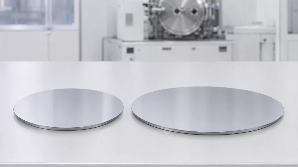
This guide compares 4-inch and 6-inch sapphire substrates from a practical purchasing and production perspective.
Quick Comparison
| 항목 | 4-Inch Sapphire Substrate | 6-Inch Sapphire Substrate |
|---|---|---|
| Common nominal diameter | 100mm | 150mm |
| Nominal surface area | Approximately 78.5 cm² | Approximately 176.7 cm² |
| Area ratio | 1.00 | Approximately 2.25 |
| Common thickness range | Often around 650 μm | Often around 1,000–1,300 μm |
| Handling risk per wafer | Lower | Higher financial loss if one wafer breaks |
| Geometry control | Generally easier | More demanding across the larger diameter |
| Thermal bow sensitivity | Important | Usually more critical |
| Edge-loss percentage | Higher for the same exclusion width | Lower for the same exclusion width |
| Equipment availability | Widely supported in development and production | Requires a qualified 150 mm process line |
| Best suited for | R&D, pilot production and flexible sourcing | Qualified high-volume manufacturing |
These values are general market references rather than universal specifications. Actual diameter, thickness and geometry limits must be confirmed against the MOCVD reactor, wafer carrier, lithography system and downstream process.
Confirm the Actual Diameter Before Comparing Prices
“4-inch” and “6-inch” are often used as nominal size descriptions. They do not always define the exact mechanical diameter.
Depending on the supplier and equipment platform, a quotation may refer to:
- 100.0 mm or 101.6 mm for a nominal 4-inch wafer
- 150.0 mm or 152.4 mm for a nominal 6-inch wafer
A difference of several millimeters can affect wafer pockets, cassettes, transfer robots, alignment and edge clearance.
A complete RFQ should state the required diameter in millimeters, including tolerance. It should also identify whether the wafer uses a primary flat, secondary flat or notch.
Understanding TTV
Total thickness variation, or TTV, is the difference between the maximum and minimum measured thickness within the defined inspection area.
TTV is not the same as bow. A sapphire wafer may have relatively uniform thickness while still being curved. It may also appear flat but have unacceptable local thickness variation.
Why TTV Matters in GaN Epitaxy
TTV can influence:
- Wafer-to-susceptor contact
- Temperature distribution across the substrate
- Film-thickness uniformity
- Lithography focus
- Patterned sapphire substrate processing
- Backgrinding and dicing stability
- Final device wavelength or electrical uniformity
For a 6-inch substrate, controlling thickness over a 150 mm diameter is generally more demanding than controlling it over 100 mm. Buyers should therefore compare measurement methods, not only the number printed on the certificate.
Common Commercial TTV Ranges
Public commercial specifications commonly show approximate limits such as:
- 4-inch sapphire: TTV below approximately 10–20 μm
- 6-inch sapphire: TTV below approximately 10–25 μm
These are not mandatory industry-wide limits. High-uniformity epitaxy, advanced lithography or microLED processes may require tighter values.
A tighter TTV specification can increase polishing time, inspection requirements, rejection rate and substrate cost. It should therefore be connected to an actual process requirement.
Always Define the TTV Measurement Conditions
An RFQ should specify:
- Measurement tool or accepted measurement principle
- Wafer support or chucking condition
- Measurement grid or scan density
- Edge exclusion used during measurement
- Whether the result is full-wafer TTV or site-based flatness
- Whether the certificate includes a wafer map or only a maximum value
A supplier reporting TTV over a 5 mm edge exclusion cannot be directly compared with a supplier reporting over a 2 mm exclusion.
Bow: Incoming Bow and Thermal Bow Are Different
Bow generally describes the displacement of the wafer’s median surface at its center relative to a reference plane when the wafer is measured without forced flattening.
Incoming bow is normally measured at room temperature before epitaxy. Thermal bow develops while the wafer is heated and coated.
Why Thermal Bow Is Critical for GaN-on-Sapphire
GaN and sapphire have different lattice parameters and thermal expansion behavior. During high-temperature epitaxy and cooling, stress develops in the GaN-on-sapphire structure.
The final wafer shape depends on several interacting factors:
- Initial sapphire bow
- Internal stress in the sapphire crystal
- Substrate thickness
- GaN buffer-layer design
- Total epitaxial-layer thickness
- MOCVD temperature profile
- Susceptor pocket geometry
- Backside finish
- Heating and cooling rates
A substrate with acceptable room-temperature bow may still develop excessive thermal bow during epitaxy. Conversely, a slightly pre-shaped substrate may perform well with a specific epitaxial recipe.
For this reason, incoming bow alone is not sufficient for qualifying a 6-inch sapphire substrate.
Risks Associated with Excessive Bow
Excessive bow can cause:
- Uneven thermal contact
- Radial temperature variation
- Non-uniform GaN thickness
- Wavelength variation across LED wafers
- Lithography focus errors
- Edge lift inside the susceptor pocket
- Wafer slip or unstable rotation
- Cracking during cooling
- Breakage during handling or back-thinning
The effect is often more noticeable on 6-inch wafers because the larger span amplifies the consequences of curvature and thermal gradients.
Do Not Confuse Bow with Warp
Bow is mainly a center-point measurement relative to a reference plane. Warp evaluates the overall peak-to-valley deviation of the wafer’s median surface.
A wafer can meet a bow requirement while failing warp because of an asymmetric, saddle-shaped or irregular surface.
For production purchasing, it is usually safer to specify:
- TTV
- Bow
- Warp
- Measurement edge exclusion
- Free-state or supported measurement condition
Using only one geometry parameter leaves room for incompatible interpretations.
Edge Exclusion and Usable Wafer Area
Edge exclusion is the radial region near the wafer perimeter that is not included in a specific measurement or process acceptance area.
Different operations may use different exclusions:
- Geometry measurement edge exclusion
- Epitaxial uniformity edge exclusion
- Lithography edge exclusion
- Device-design keep-out zone
- Dicing and edge-chipping allowance
These values should not be treated as interchangeable.
Example: Effect of a 3 mm Radial Edge Exclusion
The following calculation uses ideal circular wafers of 100 mm and 150 mm diameter. Flats, notches, alignment losses and die layout are not included.
| 웨이퍼 크기 | Full Area | Area After 3 mm Exclusion | Usable Percentage |
| 100mm | 78.5 cm² | 69.4 cm² | 88.4% |
| 150mm | 176.7 cm² | 162.9 cm² | 92.2% |
With the same 3 mm edge exclusion, the 150 mm wafer provides approximately 2.35 times the ideal usable area of the 100 mm wafer.
This is slightly higher than the full-area ratio of 2.25 because the same exclusion width consumes a smaller percentage of the larger wafer.
Why the Edge Region Is Difficult
Near-edge process performance may be affected by:
- Edge bevel geometry
- Local wafer thickness change
- Polishing roll-off
- 엣지 치핑
- Susceptor pocket clearance
- Gas-flow disturbance
- Temperature gradients
- GaN edge deposition
- Particle accumulation
- Lithography focus limitations
A supplier should not guarantee an edge performance value without a clearly defined exclusion zone and inspection method.
Does a 6-Inch Sapphire Substrate Reduce Cost?
A 6-inch substrate usually costs more per wafer. The correct question is whether it reduces cost per usable area or cost per qualified device.
Basic Substrate Cost per Usable Area
A simple comparison is:
Substrate cost per usable area = wafer price ÷ usable wafer area
If a 6-inch wafer costs less than 2.25 times the price of a 4-inch wafer and both provide equal full-area yield, its raw substrate cost per square centimeter may be lower.
However, this calculation does not include epitaxy and downstream losses.
Effective Cost per Good Area
A more useful model is:
Effective cost per good area = total processed wafer cost ÷ (usable area × epitaxy yield × device-process yield)
Total processed wafer cost may include:
- Sapphire substrate
- MOCVD processing
- Patterned substrate processing
- Photolithography
- Deposition and etching
- Backgrinding
- Laser lift-off, when applicable
- Dicing
- Inspection
- Equipment conversion
- Breakage and rejected wafers
A larger wafer is economically attractive only when the complete process remains stable.
Cost Advantages of 6-Inch Sapphire
Potential advantages include:
- Approximately 2.25 times the nominal area per wafer
- Lower edge-loss percentage
- More devices per handling cycle
- Improved automation efficiency
- Better alignment with 150 mm semiconductor equipment
- Lower labor and packaging cost per unit area
- Potentially lower epitaxy cost per device
Hidden Costs of Moving to 6-Inch
Possible additional costs include:
- New or modified MOCVD susceptors
- 150 mm cassettes and carriers
- Robot and aligner qualification
- Lithography recipe conversion
- New dicing or thinning fixtures
- Higher-value loss when one wafer breaks
- Longer supplier qualification
- Increased demand for geometry and cleanliness control
- Yield loss during early production stages
A 6-inch conversion should therefore be evaluated as a production-line project, not merely as a substrate-price comparison.
Compare Reactor Throughput by Area, Not Wafer Count
A reactor may process fewer 6-inch wafers than 4-inch wafers per run. That does not necessarily mean lower throughput.
Calculate the total usable substrate area per run:
Usable area per run = wafer quantity per run × usable area per wafer
Then apply the actual epitaxial yield and cycle time.
The comparison should include:
- Wafers per reactor run
- Usable area per wafer
- Growth time
- Cleaning frequency
- Wafer loading and unloading time
- Across-wafer uniformity
- Wafer-to-wafer repeatability
- Qualified output per month
The most useful commercial metric is qualified device area per reactor hour, not simply wafer quantity.
When Should Buyers Choose 4-Inch Sapphire?
A 4-inch sapphire substrate is often a practical choice when:
- The project is in research or process-development stage
- Required quantities are relatively low
- Existing equipment is designed for 100 mm wafers
- Multiple off-cuts, thicknesses or surface options must be tested
- The epitaxial structure has not been fully stabilized
- Lower financial exposure per experimental wafer is preferred
- Flexible sourcing and shorter qualification are important
Four-inch substrates can reduce the cost of failed experiments and make it easier to compare different buffer-layer or surface-preparation conditions.
When Does 6-Inch Sapphire Make More Sense?
A 6-inch sapphire substrate becomes more attractive when:
- The MOCVD reactor is already qualified for 150 mm wafers
- Monthly production volume is high
- The epitaxial recipe has stable thermal-bow control
- Downstream tools accept the same wafer geometry
- Yield data supports the larger format
- The supplier can provide consistent lot-to-lot geometry
- Cost is evaluated per good device rather than per wafer
- Wafer maps and traceability are available
For LED and microLED production, 6-inch sapphire can offer meaningful throughput and usable-area advantages, but only after substrate and process uniformity are proven.
Suggested RFQ Starting Points
The following table is an RFQ starting framework rather than a universal acceptance standard.
| 매개변수 | 4-Inch Starting Point | 6-Inch Starting Point | Purchasing Note |
| Actual diameter | 100.0 mm with agreed tolerance | 150.0 mm with agreed tolerance | Do not order using inch description alone |
| 오리엔테이션 | C-플레인(0001) | C-플레인(0001) | State exact Miller index |
| Off-cut | Define angle, tolerance and direction | Define angle, tolerance and direction | Match the qualified GaN recipe |
| Typical thickness | Around 650 μm | Around 1,000–1,300 μm | Confirm susceptor pocket depth |
| TTV | Agree according to process, commonly ≤10–20 μm | Agree according to process, commonly ≤10–25 μm | State measurement exclusion |
| Bow | Specify maximum and sign convention | Specify maximum and sign convention | Request free-state measurement |
| Warp | Specify separately | Specify separately | Do not assume bow covers warp |
| Front surface | Epi-ready CMP | Epi-ready CMP | Define Ra and inspection method |
| Back surface | Ground, lapped or polished | Ground, lapped or polished | Match temperature-control method |
| Edge profile | Beveled and polished as required | Beveled and polished as required | Define chip acceptance criteria |
| 에지 제외 | Define for each measurement | Define for each measurement | Separate metrology and device exclusions |
| Flat or notch | Match equipment drawing | Match equipment drawing | Include orientation and dimensions |
| 청소 | Epi-ready final clean | Epi-ready final clean | Define particle requirement |
| Packaging | Individual or cassette | Individual or cassette | Confirm 100 mm or 150 mm carrier |
| Inspection report | CoA and optional wafer map | CoA and wafer map recommended | Lot traceability is important |
Important Additional Specifications
Crystal Orientation and Off-Cut
GaN epitaxy commonly uses C-plane sapphire, but off-cut angle and direction can influence surface-step structure, nucleation and epitaxial morphology.
The RFQ should state:
- Surface plane
- Off-cut angle
- Off-cut tolerance
- Off-cut direction
- Orientation measurement method
Writing only “C-plane sapphire” is not always sufficient.
Front-Surface Roughness
An epi-ready sapphire surface normally requires CMP finishing with sub-nanometer roughness. The buyer should specify:
- Ra or RMS value
- AFM scan size
- Number and location of measurement sites
- Scratch, pit and stain limits
- Cleaning condition before measurement
A very low roughness value from one small AFM scan does not describe the cleanliness or defect condition of the entire wafer.
Backside Condition
Backside finish affects:
- Thermal contact with the susceptor
- Optical pyrometry
- Wafer friction
- Particle generation
- Bow behavior
- Vacuum chucking
A ground backside and a polished backside can behave differently in the same epitaxial tool. The finish should follow the qualified production recipe rather than being selected only by appearance.
Edge Bevel and Chipping
Six-inch sapphire wafers contain more material and represent a higher value per piece. Edge damage can propagate during high-temperature processing or mechanical handling.
The RFQ should define:
- Bevel profile
- Edge polishing condition
- Maximum chip length, width and depth
- Whether chips are allowed inside the exclusion zone
- Inspection magnification
- Rejection rules for cracks
Qualification Plan for Switching from 4-Inch to 6-Inch
A controlled qualification plan should include the following stages.
Stage 1: Incoming Substrate Evaluation
Inspect:
- Diameter and thickness
- TTV, bow and warp
- 표면 거칠기
- Edge profile
- Particles and surface defects
- Crystal orientation
- Off-cut angle
- Lot traceability
Stage 2: Blank Thermal Cycle
Where practical, run uncoated substrates through a representative heating and cooling cycle. Measure wafer shape before and after the cycle to identify permanent deformation or unstable material behavior.
Stage 3: GaN Epitaxy Trial
Evaluate:
- In-situ curvature
- Temperature distribution
- GaN thickness uniformity
- Sheet resistance, when applicable
- Photoluminescence wavelength uniformity
- Cracking and edge deposition
- Final bow and warp
Stage 4: Downstream Process Verification
Confirm compatibility with:
- Lithography
- PSS processing
- Wafer bonding
- Backgrinding
- Laser processing
- Dicing
- Automated handling
Stage 5: Cost and Yield Review
Compare:
- Substrate price per usable area
- Reactor output per hour
- Good-device yield
- Breakage rate
- Rework and rejection rate
- Monthly qualified output
Only after these data are stable should the 6-inch format be treated as the lower-cost option.
Example RFQ Description
We require epi-ready C-plane sapphire substrates for GaN MOCVD growth. Please quote both 100 mm and 150 mm options. Confirm actual diameter tolerance, thickness, TTV, bow, warp, off-cut angle and direction, front-side roughness, backside finish, edge-bevel profile, particle level, packaging and inspection method. Geometry values must identify the measurement support condition and radial edge exclusion. Please provide lot-level CoA data and available wafer maps. For 150 mm substrates, please also provide information on thermal-bow control and previous GaN epitaxy qualification.
Frequently Asked Questions
Is a 6-inch sapphire substrate always cheaper per device?
No. It offers approximately 2.25 times the nominal area of a 100 mm wafer, but the economic advantage depends on wafer price, reactor configuration, usable edge area, epitaxial uniformity, downstream yield and breakage rate.
Can the same TTV specification be used for 4-inch and 6-inch wafers?
It can be requested, but achieving the same tight absolute limit over a larger diameter may increase manufacturing difficulty and price. The requirement should be based on equipment and process capability.
Is a 6-inch sapphire wafer always exactly 152.4 mm?
No. Many semiconductor suppliers use 150.0 mm for a nominal 6-inch wafer. Other applications may use 152.4 mm. The RFQ must state the exact metric diameter.
What edge exclusion should be specified?
There is no single value suitable for every process. Buyers often work with exclusions of a few millimeters, but geometry measurement, epitaxy, lithography and device layout may require different values. Each exclusion should be defined separately.
Does lower incoming bow guarantee lower bow after GaN growth?
No. Final bow depends on the substrate, GaN stack, stress evolution, temperature profile and cooling conditions. Incoming bow is only one part of the qualification.
Does moving to 6-inch automatically improve GaN crystal quality?
No. Larger diameter mainly improves potential throughput. GaN crystal quality still depends on sapphire surface condition, off-cut accuracy, buffer-layer design and epitaxial parameters.
Should buyers request SSP or DSP sapphire?
The choice depends on the MOCVD susceptor, temperature measurement method, downstream bonding and lithography requirements. The front side must be epi-ready, while the backside condition should match the qualified process.
결론
A 6-inch sapphire substrate offers a clear area advantage over a 4-inch substrate, but diameter alone does not determine production economics.
For GaN epitaxy, buyers should compare TTV, bow, warp, thermal-bow behavior, edge exclusion, backside finish and equipment compatibility. A 4-inch wafer often remains the safer choice for development and low-volume production, while a qualified 6-inch platform can improve usable area, automation efficiency and cost per device in high-volume manufacturing.
The most reliable purchasing decision is based on qualified output per reactor hour and cost per good device—not wafer price alone.