
As semiconductor technology advances toward smaller process nodes, larger wafer sizes, and increasingly complex manufacturing environments, material selection has become a critical engineering consideration. Modern semiconductor equipment operates under extreme conditions involving ultra-high temperatures, plasma exposure, corrosive process gases, vacuum environments, and strict contamination requirements. Under such conditions, conventional engineering materials often struggle to meet performance demands.
Among the most important advanced materials used throughout semiconductor manufacturing are technical ceramics, synthetic sapphire, and silicon carbide (SiC). Although these materials are sometimes grouped together because of their high-temperature capabilities and chemical stability, their performance characteristics differ significantly.
Understanding the distinctions and relationships among ceramics, sapphire, and silicon carbide helps engineers optimize equipment design, improve process stability, and reduce contamination risks.
Understanding the Three Material Categories
Before comparing performance, it is important to understand that these materials belong to different categories.
Advanced Ceramics
Advanced ceramics are engineered inorganic materials manufactured through controlled powder processing and sintering techniques.
Common semiconductor ceramic materials include:
- Alumina (Al₂O₃)
- Aluminum Nitride (AlN)
- Zirconia (ZrO₂)
- Silicon Nitride (Si₃N₄)
- Boron Nitride (BN)
These materials are selected according to specific thermal, mechanical, and electrical requirements.
사파이어
Sapphire is a single-crystal form of aluminum oxide (Al₂O₃). Although chemically related to alumina ceramics, sapphire possesses a highly ordered crystal structure rather than a polycrystalline microstructure.
This distinction results in:
- superior optical transmission
- lower porosity
- greater purity consistency
- exceptional surface quality
Synthetic sapphire is widely used in optical and precision semiconductor applications.
실리콘 카바이드(SiC)
Silicon carbide is an advanced ceramic compound consisting of silicon and carbon.
SiC exhibits:
- extremely high hardness
- outstanding thermal conductivity
- excellent plasma resistance
- exceptional mechanical strength
In semiconductor manufacturing, SiC increasingly serves both as a structural material and as a semiconductor substrate material.
Material Property Comparison
The differences become clearer when key engineering properties are compared.
| 속성 | Advanced Ceramics | 사파이어 | 실리콘 카바이드 |
|---|---|---|---|
| Main Composition | Various oxides/nitrides | Single-crystal Al₂O₃ | SiC |
| Density (g/cm³) | 3–6 | 3.98 | 3.21 |
| 경도(Mohs) | 7–9 | 9 | 9–9.5 |
| Maximum Service Temperature | 1400–1700°C | ~1800–2000°C | >1600°C |
| 열 전도성 | 보통 | 보통 | Extremely High |
| Plasma Resistance | Good | 보통 | 우수 |
| 광학 투명도 | 제한적 | 우수 | Poor |
| 내식성 | 우수 | 우수 | 우수 |
| 전기적 특성 | Adjustable | Insulator | 반도체 |
| Relative Cost | 보통 | 높음 | 높음 |
Although each material demonstrates strong performance, their strengths address different semiconductor requirements.
Thermal Performance in Semiconductor Systems
High-temperature processing remains central to semiconductor fabrication.
애플리케이션에는 다음이 포함됩니다:
- oxidation
- diffusion
- annealing
- 에피택시
- 화학 기상 증착
Material thermal performance directly affects process reliability.
Advanced Ceramics
Materials such as alumina and aluminum nitride provide stable operation at elevated temperatures.
Advantages include:
- 열 안정성
- electrical insulation
- structural rigidity
However, thermal conductivity varies significantly between ceramic types.
사파이어
Sapphire exhibits excellent temperature resistance and dimensional stability.
Its low thermal expansion supports precision optical systems.
However, sapphire generally dissipates heat less efficiently than SiC.
실리콘 카바이드
SiC offers exceptionally high thermal conductivity.
This enables:
- 빠른 열 방출
- improved temperature uniformity
- reduced thermal gradients
As wafer sizes continue increasing, thermal management advantages become increasingly valuable.
Plasma Resistance and Etching Environments
Plasma processes create highly aggressive operating environments.
Energetic ions continuously bombard internal chamber surfaces.
Material degradation can lead to:
- contamination
- particle generation
- process drift
- reduced tool uptime
Silicon Carbide Leads in Plasma Resistance
Silicon carbide demonstrates superior resistance to plasma erosion.
As a result, SiC is widely used for:
- focus rings
- chamber liners
- edge rings
- etch hardware
Advanced Ceramics
Some ceramic materials also provide excellent plasma performance.
Yttria-containing ceramics are increasingly used in plasma chambers.
사파이어
Although sapphire remains chemically stable, prolonged plasma exposure may gradually degrade surfaces under certain process conditions.
Therefore, sapphire is generally selected for optical rather than plasma-facing applications.
Optical Applications
Optical transparency represents another major distinction.
Sapphire Advantages
Sapphire transmits light over a broad wavelength range extending from ultraviolet through infrared.
애플리케이션에는 다음이 포함됩니다:
- 광학 창
- viewport assemblies
- laser systems
- wafer inspection systems
- sensor components
Its combination of transparency and durability is difficult to replicate.
Ceramics and SiC Limitations
Most ceramic materials and SiC are opaque.
Consequently, they cannot replace sapphire in optical systems.
Contamination and Cleanliness Considerations
Semiconductor manufacturing requires extremely low particle generation.
Material wear and surface degradation directly influence yield.
Advanced Ceramics
Properly engineered ceramics generate minimal contamination.
However, porosity and grain boundaries may affect performance.
사파이어
Single-crystal sapphire provides:
- very low porosity
- smooth polished surfaces
- excellent cleanliness characteristics
실리콘 카바이드
SiC also demonstrates excellent contamination performance due to high wear resistance and chemical stability.
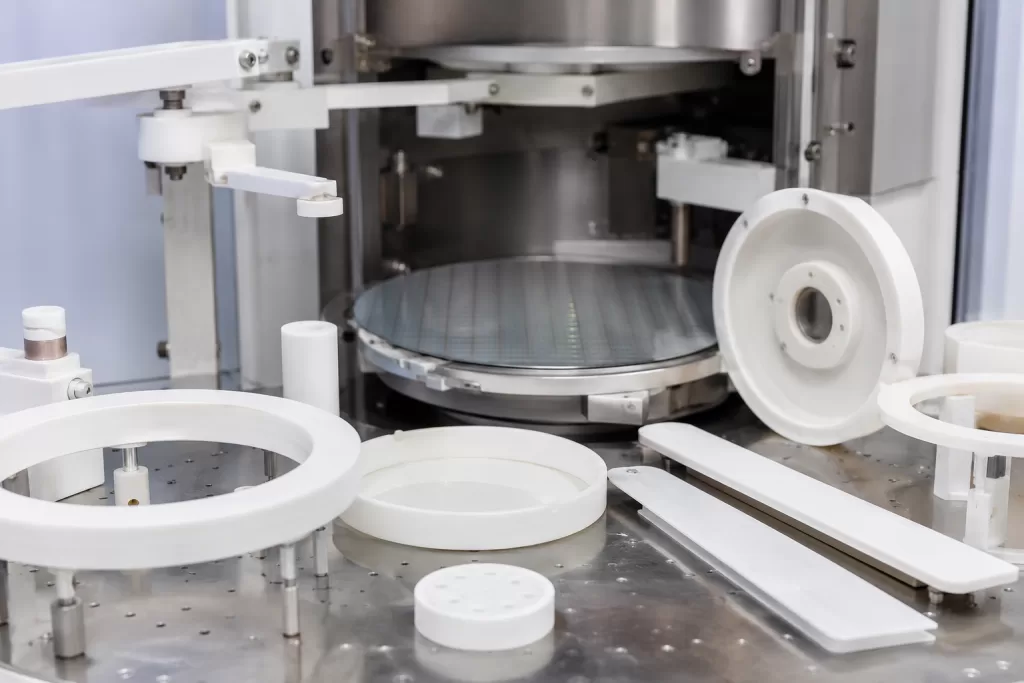
Typical Semiconductor Applications
Each material category occupies specific roles inside fabrication systems.
| 재료 | Common Semiconductor Applications |
|---|---|
| Advanced Ceramics | Insulators, wafer chucks, structural components |
| 사파이어 | Optical windows, precision bearings, sensor components |
| 실리콘 카바이드 | Etching hardware, focus rings, wafer susceptors, substrate materials |
Rather than competing directly, these materials frequently complement one another within equipment systems.
Future Material Trends
As semiconductor manufacturing progresses toward sub-2nm process nodes, materials continue evolving.
Emerging developments include:
- plasma-resistant ceramic coatings
- ultra-high purity ceramic systems
- larger SiC structural components
- sapphire precision assemblies
- ceramic composite materials
- advanced contamination control technologies
Future fabrication tools will increasingly rely on specialized materials optimized for individual process environments.
결론
Although ceramics, sapphire, and silicon carbide are all considered advanced engineering materials, they serve distinct roles within semiconductor manufacturing.
Advanced ceramics provide versatile structural and electrical solutions. Sapphire excels in optical and precision applications. Silicon carbide dominates high-temperature and plasma-intensive environments.
Rather than replacing one another, these materials work together to support modern semiconductor equipment performance. Selecting the appropriate material depends on operating conditions, contamination requirements, thermal considerations, and process objectives.
As semiconductor technologies continue advancing, understanding these material differences will remain essential for both equipment manufacturers and process engineers.
자주 묻는 질문
Is sapphire considered a ceramic?
Chemically, sapphire is aluminum oxide like alumina ceramic, but sapphire is a single-crystal material rather than a polycrystalline ceramic.
Why is silicon carbide increasingly important in semiconductor manufacturing?
SiC offers outstanding thermal conductivity, plasma resistance, and mechanical strength, making it highly suitable for advanced process environments.
Which material is best for semiconductor equipment?
There is no universally best material. Selection depends on application requirements such as temperature, optical performance, contamination control, and plasma exposure.